Semiconductor wafer mounting method and semiconductor wafer mounting apparatus

Inactive Publication Date: 2012-11-29
NITTO DENKO CORP
View PDF1 Cites 5 Cited by
  • Summary
  • Abstract
  • Description
  • Claims
  • Application Information

AI Technical Summary

Benefits of technology

[0008]This invention has been made regarding the state of the art noted above, and its primary object is to provide a semiconductor wafer mounting method and a semiconductor wafer mounting apparatus

Problems solved by technology

As a result, the following problem may arise.
Consequently, the following problems may arise.
In this case, there aris

Method used


Image

  • Semiconductor wafer mounting method and semiconductor wafer mounting apparatus
  • Semiconductor wafer mounting method and semiconductor wafer mounting apparatus
  • Semiconductor wafer mounting method and semiconductor wafer mounting apparatus

Examples


Example

[0060]The invention is described more fully hereinafter with reference to the accompanying drawings, in which embodiments of the invention are shown. This invention may, however, be embodied in many different forms and should not be construed as limited to the embodiments set forth herein. Rather, these embodiments are provided so that this disclosure is thorough, and will fully convey the scope of the invention to those skilled in the art. In the drawings, the size and relative sizes of layers and regions may be exaggerated for clarity. Like reference numerals in the drawings denote like elements.

[0061]One embodiment of this invention will be described hereunder with reference to the drawings.

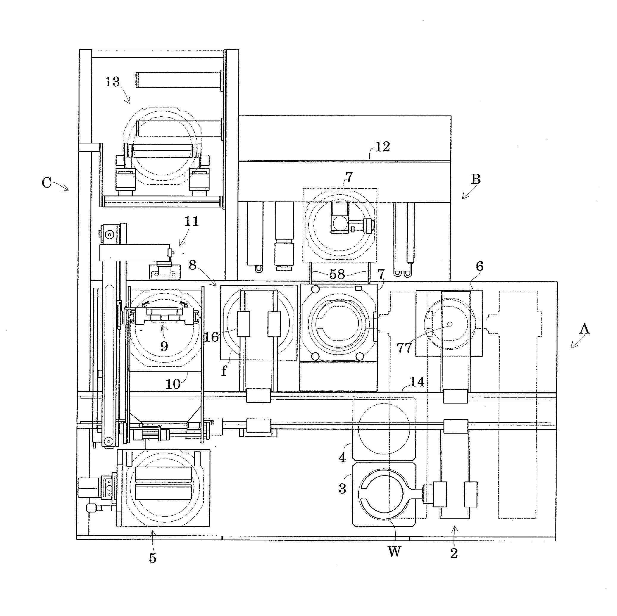
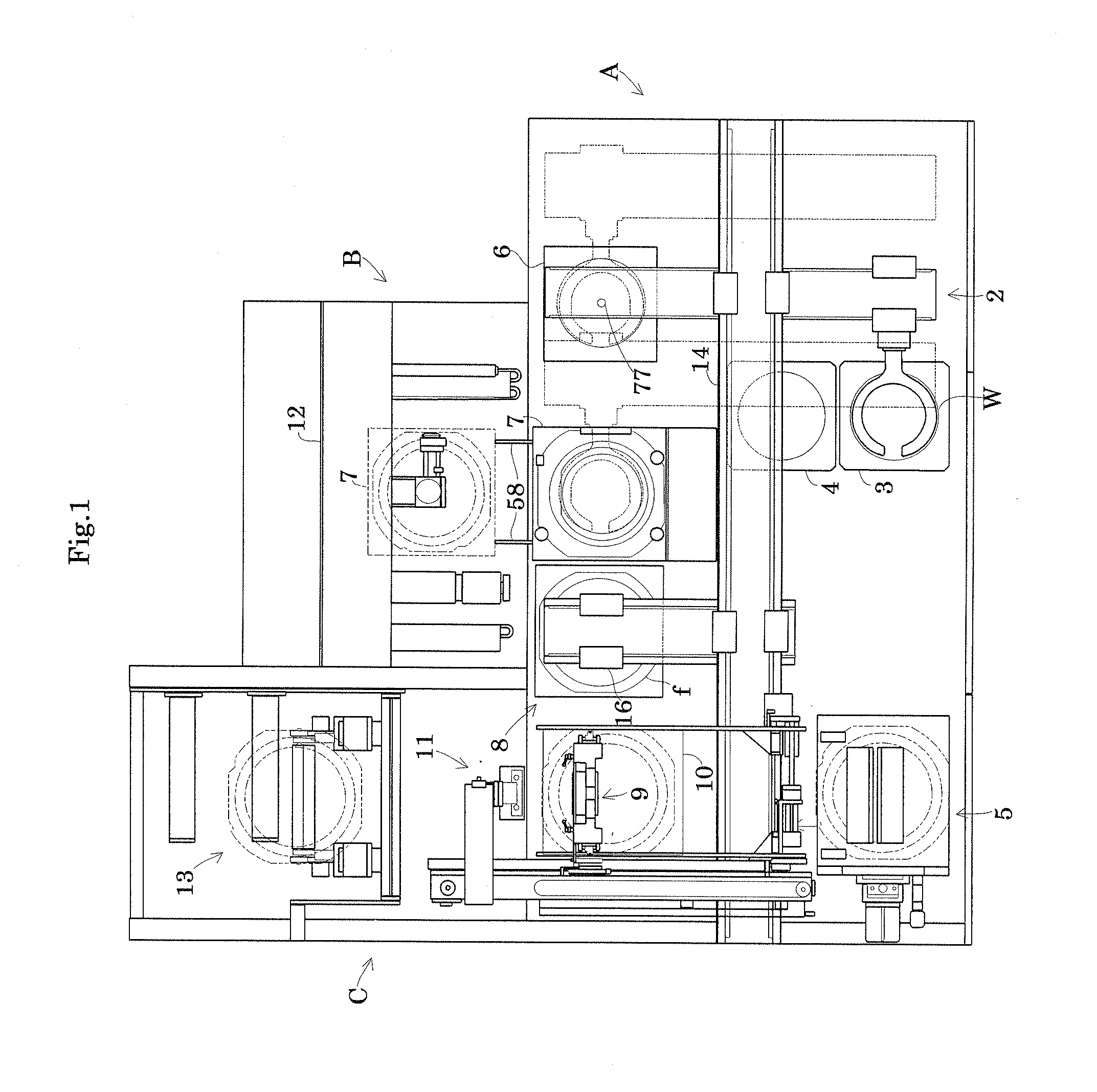
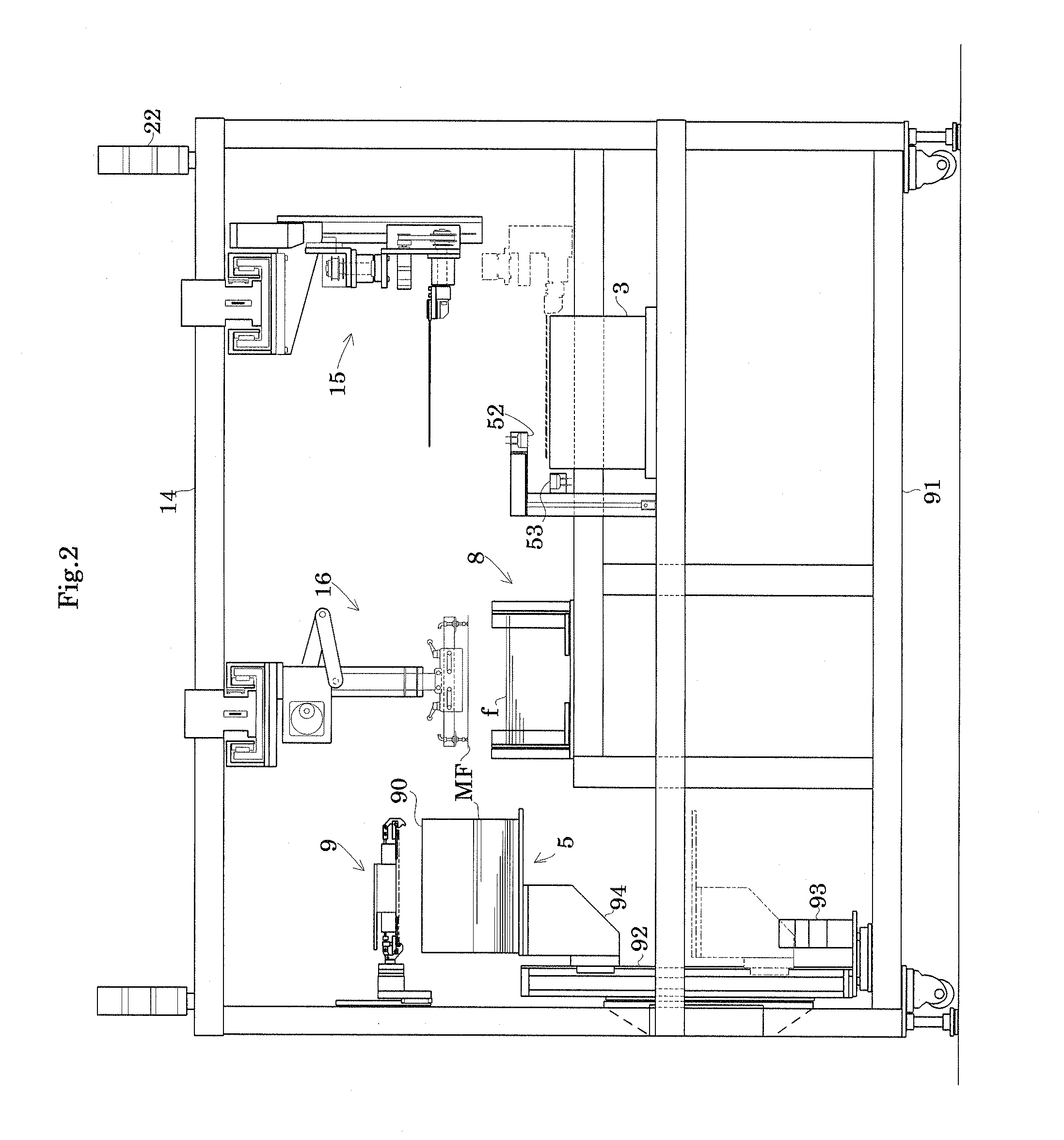
[0062]FIG. 1 shows a plan view of a semiconductor wafer mounting apparatus, and FIG. 2 a front view thereof.

[0063]As shown in FIG. 1, the semiconductor wafer mounting apparatus includes a basic unit with a laterally extending rectangular section A and a protrusion section B connected to on a c...


PUM

PropertyMeasurementUnit
Permeabilityaaaaaaaaaa

Abstract

A workpiece is unloaded from a wafer-receiving container. A first discriminating sensor detects a front surface of the workpiece, and determines either a semiconductor wafer or a spacer is the workpiece. Where the workpiece is a wafer, the first discriminating sensor also determines whether or not a protective tape is on the front surface of the workpiece. Where it is determined that a protective tape is not on the front surface, a second discriminating sensor detects a back surface of the wafer for discriminating the presence or absence of the protective tape.

Description

BACKGROUND OF THE INVENTION[0001]1. Field of the Invention[0002]This invention relates to a semiconductor wafer mounting method and a semiconductor wafer mounting apparatus in which a semiconductor wafer (hereinafter, appropriately referred to as a “wafer”) subjected to a back grinding process that is stacked via a spacer such as an inserting paper in a receiving container is unloaded from the container, and then is mounted onto a ring frame via a supporting adhesive tape.[0003]2. Description of the Related Art[0004]A plurality of semiconductor wafers and spacers are alternately stacked in a container for transporting the semiconductor wafers to every process. When the semiconductor wafer is transported out of the container with a front surface thereof being suction-held, the spacer on a back surface side of the semiconductor wafer adheres to a back surface of the semiconductor wafer due to static electricity. Then a spacer retaining mechanism is provided for separating the spacer f...

Claims


Application Information

Patent Timeline
IPC IPC(8): B29C65/50
CPCH01L21/67132B29C65/50
Inventor YAMAMOTO, MASAYUKIOKUNO, CHOUHEI
Owner NITTO DENKO CORP
Why Eureka
Try Eureka