
Light source device and image display apparatus

Inactive Publication Date: 2012-11-29
PANASONIC INTELLECTUAL PROPERTY MANAGEMENT CO LTD
View PDF12 Cites 24 Cited by
  • Summary
  • Abstract
  • Description
  • Claims
  • Application Information

AI Technical Summary

Benefits of technology

[0008]The present invention has been made in view of such a conventional problem, and an objective of the present invention is to provide a light source device that is highly reliable due to having an extended lifespan as a result of a reduction in variation of lifespan among multiple semiconductor laser light sources, and an image display apparatus including the light source device.
[0034]With the present invention, variation of lifespan among the multiple semiconductor laser light sources can be reduced, and lifespan of the light source device can be extended. Thus, a highly reliable light source device, and an image display apparatus including the light source device can be provided.

Problems solved by technology

However, cooling unevenness that occurs among multiple light sources cannot be solved by the image projection device disclosed in Japanese Laid-Open Patent Publication No. 2009-31622.
Thus, the problem regarding reduced lifespan of the light source device caused by the variation in lifespan among the multiple light sources cannot be solved.

Method used


Image

  • Light source device and image display apparatus
  • Light source device and image display apparatus
  • Light source device and image display apparatus

Examples


first embodiment

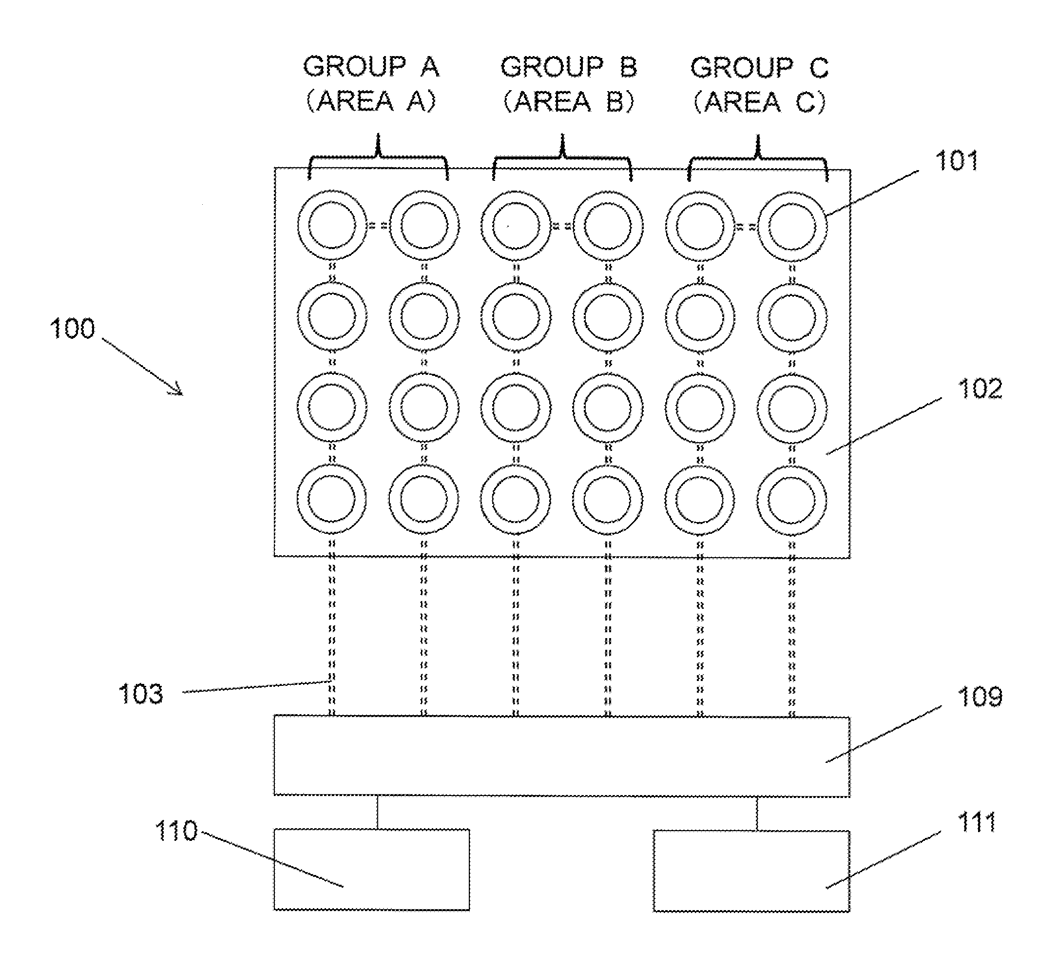
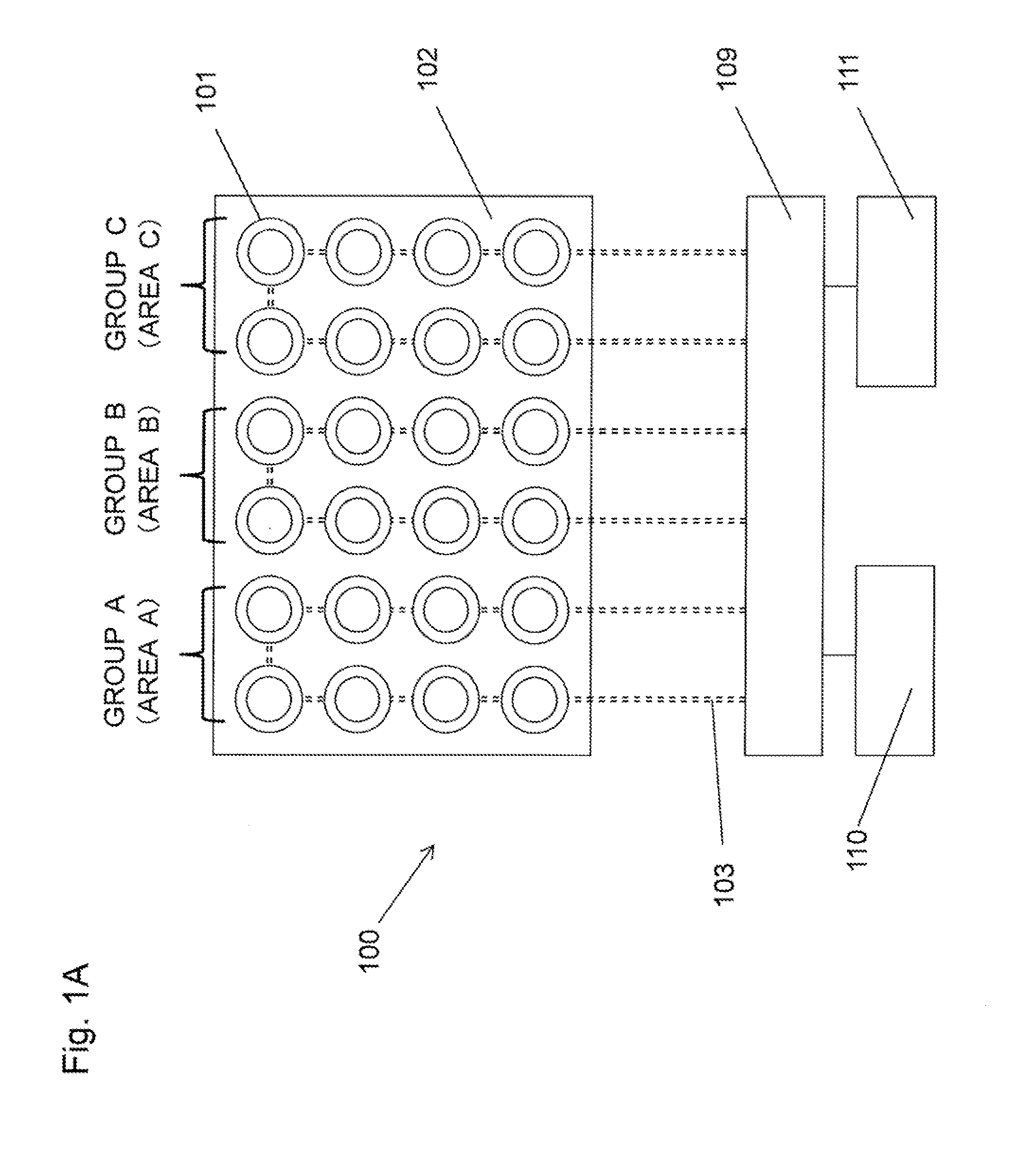
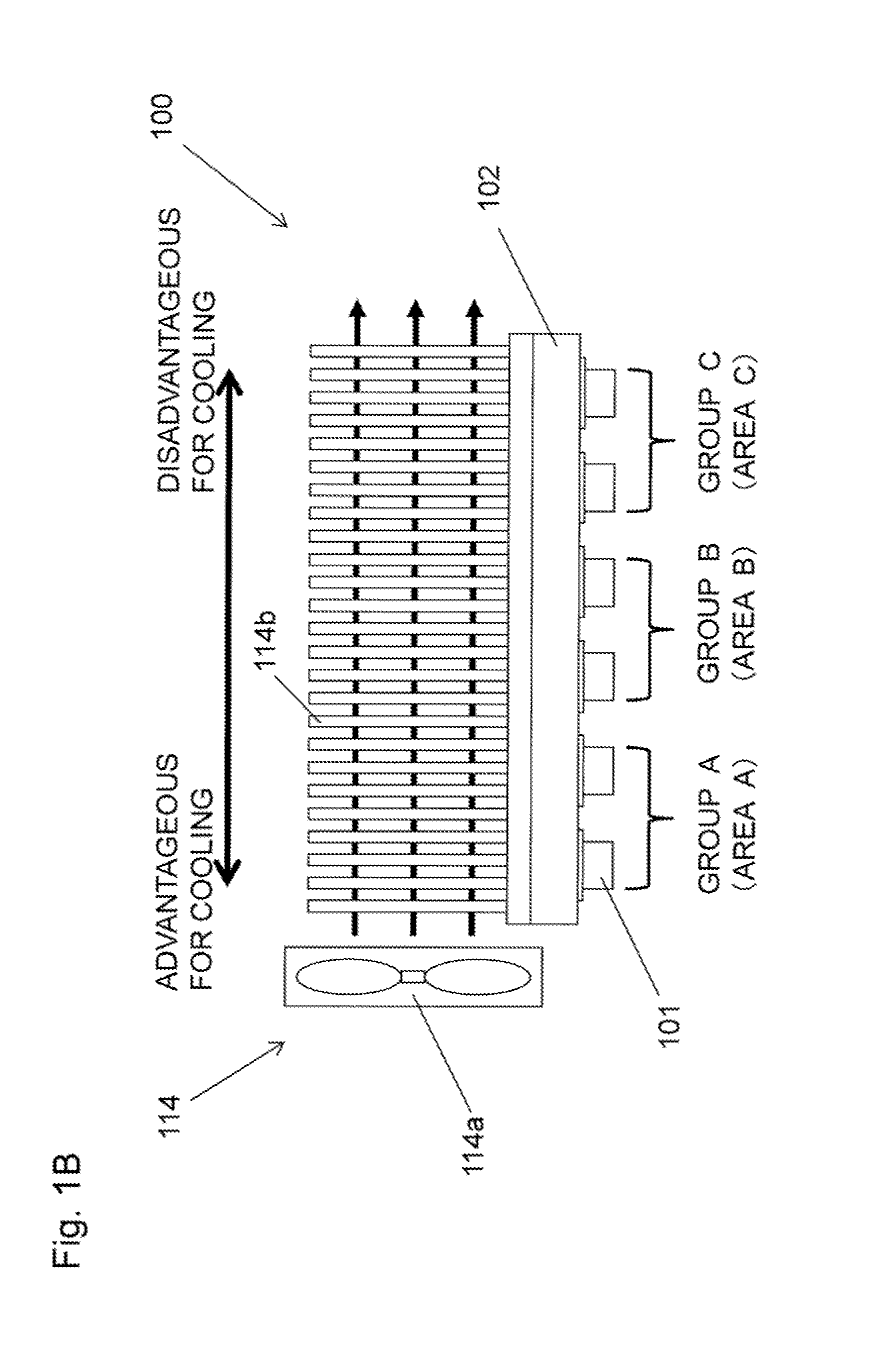
[0045]In the following, a light source device of the present embodiment will be described with reference to the drawings. FIG. 1A is a front view of a light source device 100 according to the present embodiment. FIG. 1B is a side view of the light source device 100 according to the present embodiment. FIG. 2 is an illustrative diagram of semiconductor laser light sources 101 according to the present embodiment; and FIG. 2(a) is an illustrative diagram of a light-emitting surface side of the semiconductor laser light sources 101, and FIG. 2(b) is an illustrative diagram of a rear surface side thereof. FIG. 3 is an illustrative diagram of a base plate 102 according to the present embodiment.

[0046]As shown in FIG. 1A, the light source device 100 according to the present embodiment includes: the multiple semiconductor laser light sources 101; the base plate 102 having thereon an installation area on which the multiple semiconductor laser light sources 101 are installed and which is divi...

second embodiment

[0070]In the following, a light source device 200 according to the present embodiment will be described with reference to FIG. 4. FIG. 4 is an illustrative diagram of the light source device 200 according to the present embodiment.

[0071]As shown in FIG. 4, in the light source device 200 according to the present embodiment, the number of the semiconductor laser light sources 101 belonging to a group is eight for group A as similar to that in the first embodiment, but is six for group B, and is four for group C. Except for the above described point, the components are identical to those of the first embodiment, and reference characters identical to those in the first embodiment are provided thereto and descriptions of those are omitted. As shown in FIG. 4, the number of the semiconductor laser light sources 101 arranged per unit area is smaller for a group arranged at a leeward position that is difficult to be cooled than a group arranged at a windward position. With this, the amount ...

third embodiment

[0074]In the following, a light source device according to the present embodiment will be described with reference to FIG. 5. As shown in FIG. 5, in a light source device 300 according to the present embodiment, a light source-installed part, where the semiconductor laser light sources 101 are arranged, is formed on multiple base plates that are thermally isolated from each other (in FIG. 5, an example is shown in which two base plates of a base plate 301 and a base plate 302 are provided). In other words, the multiple base plates are separately arranged. Except for the above described point, the components are identical to those of the first embodiment, and reference characters identical to those in the first embodiment are provided thereto and descriptions of those are omitted.

[0075]In the present embodiment, multiple base plates are provided. On each of the base plates (the base plate 301 and the base plate 302), at least one group including at least one of the semiconductor lase...


PUM


Abstract

A light source device 100 includes: multiple semiconductor laser light sources 101; a base plate 102 having thereon an installation area on which the multiple semiconductor laser light sources 101 are installed and which is divided into multiple areas, thus dividing the multiple semiconductor laser light sources 101 on the installation area into the multiple groups such that each of the groups includes one of the multiple semiconductor laser light sources 101 or at least two of the semiconductor laser light sources 101 that are electrically connected in series; and a current control section 109 configured to conduct temperature control of the semiconductor laser light sources 101 by independently controlling a value of current flowing in each of the groups of the multiple semiconductor laser light sources 101 on the installation area.

Description

BACKGROUND OF THE INVENTION[0001]1. Field of the Invention[0002]The present invention relates to a light source device, and an image display apparatus including the light source device.[0003]2. Description of the Background Art[0004]Hitherto, for example, there are cases where a solid light source such as a semiconductor laser light source and the like is used in an image display apparatus such as a projector and the like. In such cases, when a state of the light source being at a high temperature continues for a long period of time, a problem arises where an optical output of the light source deteriorates. In order to avoid such a problem, typically, a cooling device such as a heat sink and the like and a cooling fan and the like are used for cooling. As a result, a state of the semiconductor laser light source being at a high temperature, and a state of exposing, to a high temperature, a base plate on which the light source is disposed, are prevented from continuing for a long per...

Claims


Application Information

Patent Timeline
IPC IPC(8): G09G3/00F21V29/00
CPCF21V5/007F21V29/89F21V29/006F21V29/02F21V29/40F21Y2101/025H05B33/0803G09G3/001F21Y2105/003G03B21/16G03B21/2013G03B21/204G03B33/06F21V29/54F21V29/70F21V29/763F21V9/08F21Y2105/12F21Y2105/10F21Y2115/30F21Y2115/10F21K9/00F21V5/10F21V29/67H05B47/00F21S4/00F21S2/005
Inventor KITANO, HIROSHI
Owner PANASONIC INTELLECTUAL PROPERTY MANAGEMENT CO LTD
Learn More