
Semiconductor package and fabrication method thereof

a technology of semiconductors and semiconductors, applied in semiconductor devices, semiconductor/solid-state device details, electrical apparatus, etc., can solve the problems of limiting the formation of solder bumps, increasing the difficulty of forming solder bumps to joints with substrate bump pads, and reducing the process yield of the solder joint between the ic chip and the substra

Inactive Publication Date: 2012-12-13
UNIMICRON TECH CORP
View PDF11 Cites 38 Cited by
  • Summary
  • Abstract
  • Description
  • Claims
  • Application Information

AI Technical Summary

Benefits of technology

[0010]The present invention provides a method of fabricating a substrate having embedded, recessed bump pads. A core board having a first circuit pattern on its surface is provided. A dielectric layer is laminated on the core board to cover the first circuit pattern. At least a trace trench and at least a bump pad trench are in a top surface of the dielectric layer. Filling

Problems solved by technology

In other words, limitations of the solder resist opening process (approaching 60±10 μm in current processes) limits formation of the solder bumps.
The difficulty of forming solder bumps to joint with bump pads of the substrate increases for fine pitch products because of permissible alignment accuracy and small pitch between bump pads.
The small pitch between bump pads will lead to solder-climbing, decreasing process yield of the solder joint between IC chip and substrate.
Further, because solder bumps are jointed to bump pads protruding from the surface of the substrate, overflowing leading to solder bridging between bump pads, resulting in short circuiting while performing the reflow treatment, will occur because of small pitch between bump pads.

Method used


Image

  • Semiconductor package and fabrication method thereof
  • Semiconductor package and fabrication method thereof
  • Semiconductor package and fabrication method thereof

Examples


Embodiment Construction

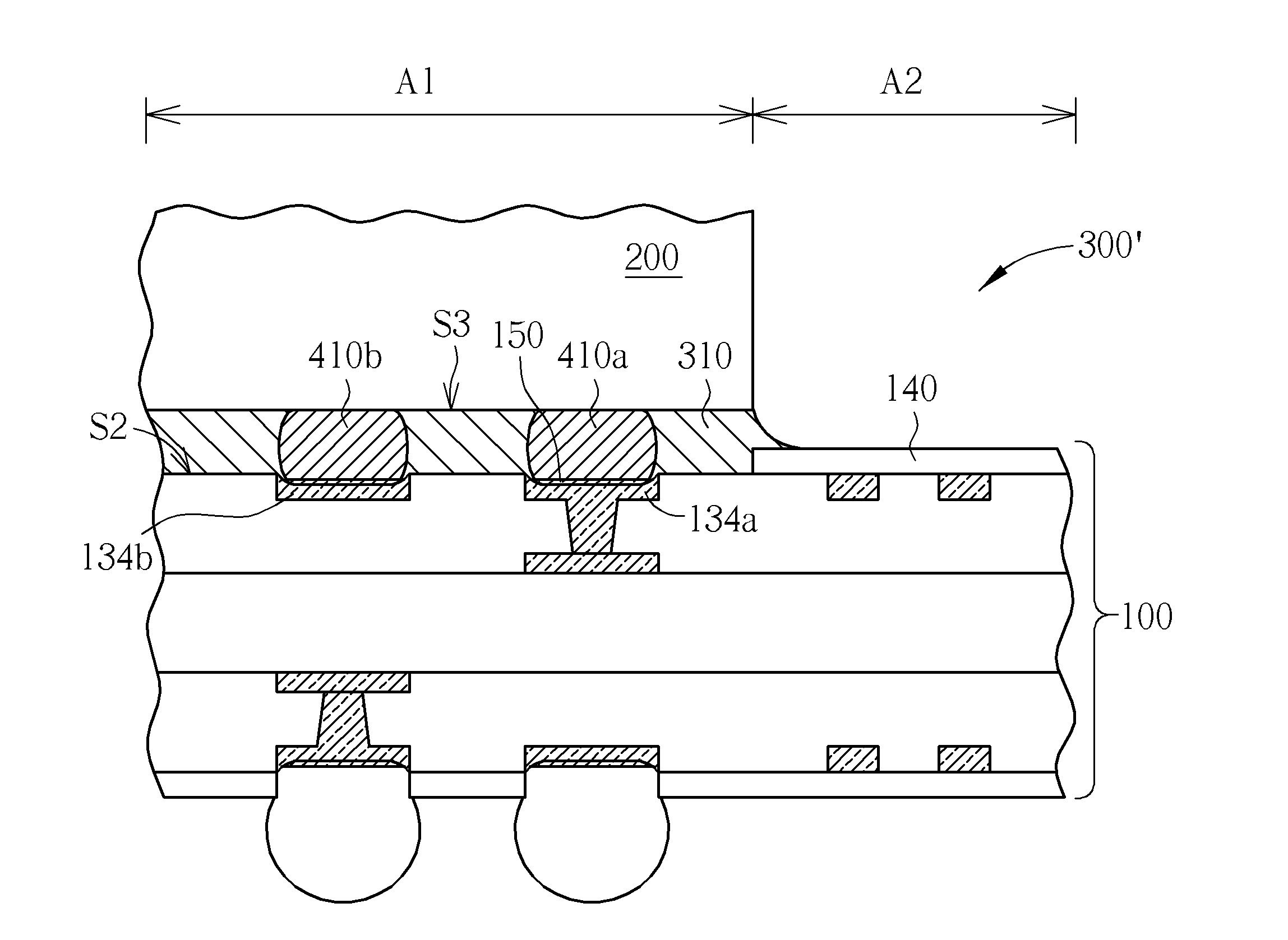
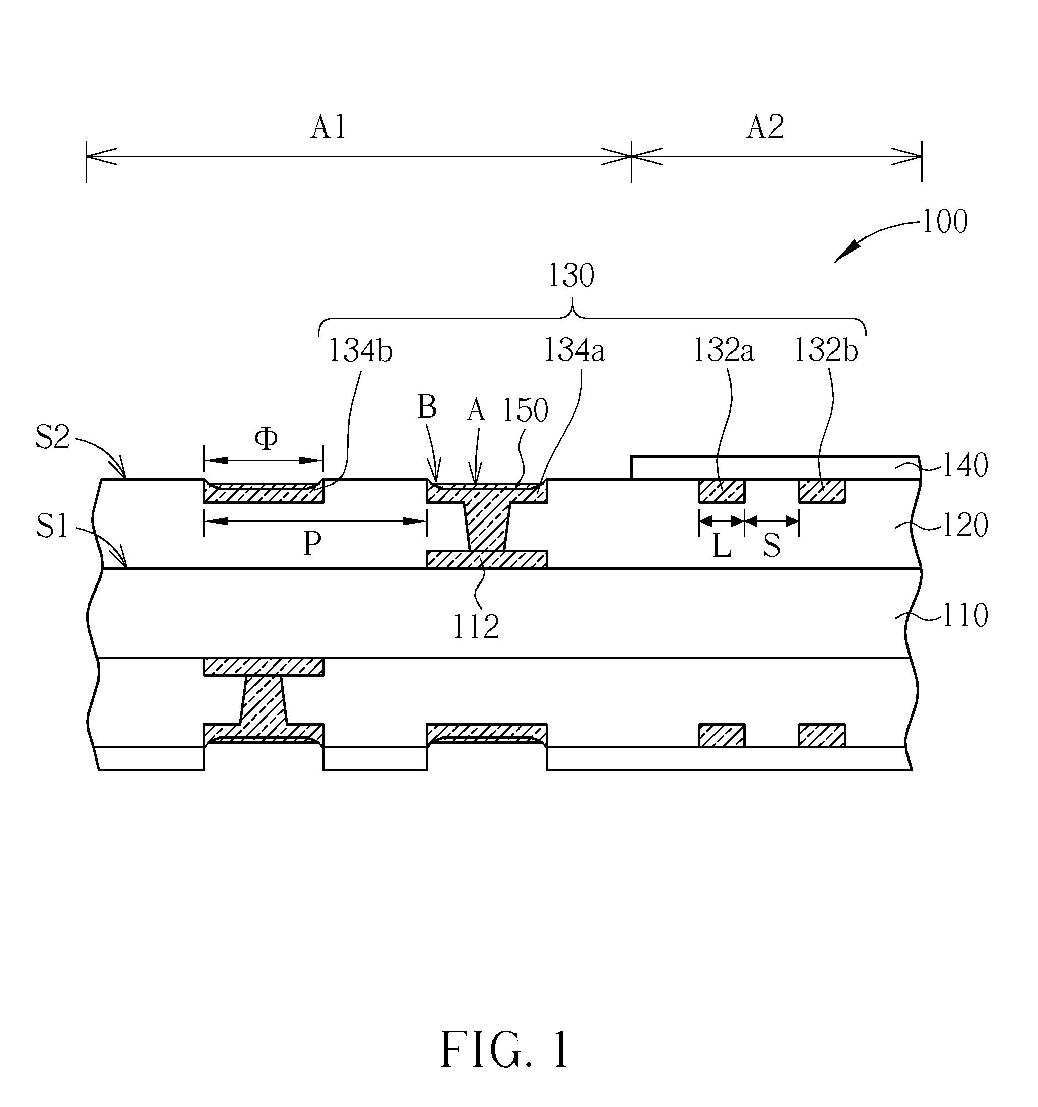
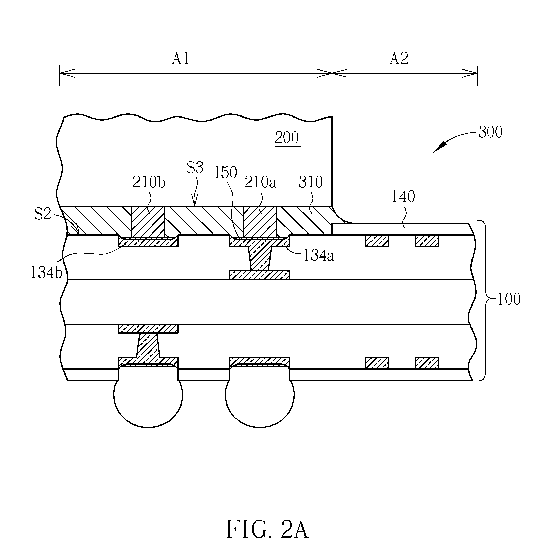
[0016]FIG. 1 schematically depicts a cross-sectional view of a substrate 100 having embedded, recessed bump pads according to one embodiment of the present invention. The substrate 100 is based on a core board 110, and multilayer circuits are gradually formed on its top and bottom sides by circuit build up technology. For simplicity, only the upper part of the substrate 100 (connected to a flip chip) is described in this embodiment, and the substrate 100 is a four-layer substrate as an example, but the substrate 100 can also be another multi-layer substrate.

[0017]To explicitly clarify the present invention, the numbers of embedded and recessed bump pads, trace trenches, bump pad trenches, circuit patterns or metal bumps disclosed in this embodiment are minimum numbers, so as to disclose the present invention clearly, but the numbers of the components are not limited. The numbers may be one or more than one, depending upon practical applications.

[0018]As shown in FIG. 1, the substrat...


PUM


Abstract

A semiconductor package includes a substrate having a flip chip bonding area. A plurality of recessed bump pads are disposed in the flip chip bonding area. The substrate further includes a solder mask that covers a circuit area. A chip having a plurality of metal bumps is mounted in the flip chip bonding area. The metal bumps are respectively connected to the recessed bump pads. An underfill is filled into the gap between the substrate and the chip.

Description

BACKGROUND OF THE INVENTION[0001]1. Field of the Invention[0002]The present invention relates generally to a semiconductor package and fabrication method thereof, and more specifically, to a semiconductor package and fabrication method thereof that apply a substrate having embedded, recessed bump pads.[0003]2. Description of the Prior Art[0004]In current semiconductor packaging technology, high-efficiency electronic components are often connected together electrically and mechanically through solder bumps and underfill injected between solder bumps. For example, an IC flip chip is usually connected to a substrate by solder bumps. This connecting technology is called flip-chip (FC) bonding technology, and is considered a type of area array bonding, which is suited for application to high density package connecting processes.[0005]The concept of the flip-chip (FC) bonding technology is to form solder bumps on electrode pads of an IC chip, reverse and put the IC flip chip on a packagin...

Claims


Application Information

Patent Timeline
IPC IPC(8): H01L23/498H01L21/60
CPCH01L2224/16225H01L2224/81411H01L23/49822H01L2224/16227H01L2224/32225H01L2224/73204H01L2924/15311H01L24/13H01L24/16H01L24/81H01L2224/13139H01L2224/13144H01L2224/13147H01L2224/13155H01L2224/16237H01L2224/81191H01L2924/00H01L2924/00014H01L2924/12042
Inventor CHENG, SHIH-LIANCHEN, TSUNG-YUAN
Owner UNIMICRON TECH CORP
Features
  • Generate Ideas
  • Intellectual Property
  • Life Sciences
  • Materials
  • Tech Scout
  • Unparalleled Data Quality
  • Higher Quality Content
  • 60% Fewer Hallucinations
Learn More