Supercharge Your Innovation With Domain-Expert AI Agents!

Touch panel

a technology of touch panel and carbon nanotube, applied in the field of touch panel, can solve the problems of poor wearability of the ito layer, uneven resistance in an entire area of the panel, and relatively complicated methods

Inactive Publication Date: 2012-12-13
SHIH HUA TECH LTD
View PDF14 Cites 13 Cited by
  • Summary
  • Abstract
  • Description
  • Claims
  • Application Information

AI Technical Summary

Problems solved by technology

However, the ITO layer is generally formed by means of ion-beam sputtering and etched by laser beam, and the method is relatively complicated.
Furthermore, the ITO layer has poor wearability, low chemical endurance and uneven resistance in an entire area of the panel.
All the above-mentioned problems of the ITO layer produce a touch panel with low sensitivity, accuracy, and brightness.

Method used


Image

  • Touch panel
  • Touch panel
  • Touch panel

Examples


Embodiment Construction

[0018]The disclosure is illustrated by way of example and not by way of limitation in the figures of the accompanying drawings in which like references indicate similar elements. It should be noted that references to “an” or “one” embodiment in this disclosure are not necessarily to the same embodiment, and such references mean at least one.

[0019]References will now be made to the drawings to describe, in detail, various embodiments of the present touch panels and method for making the same.

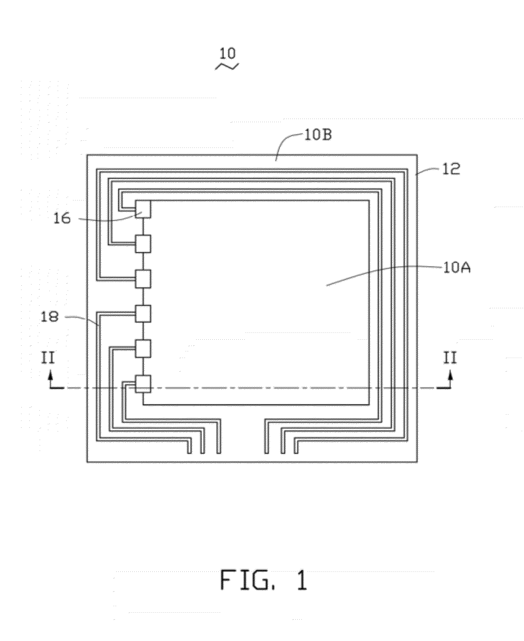
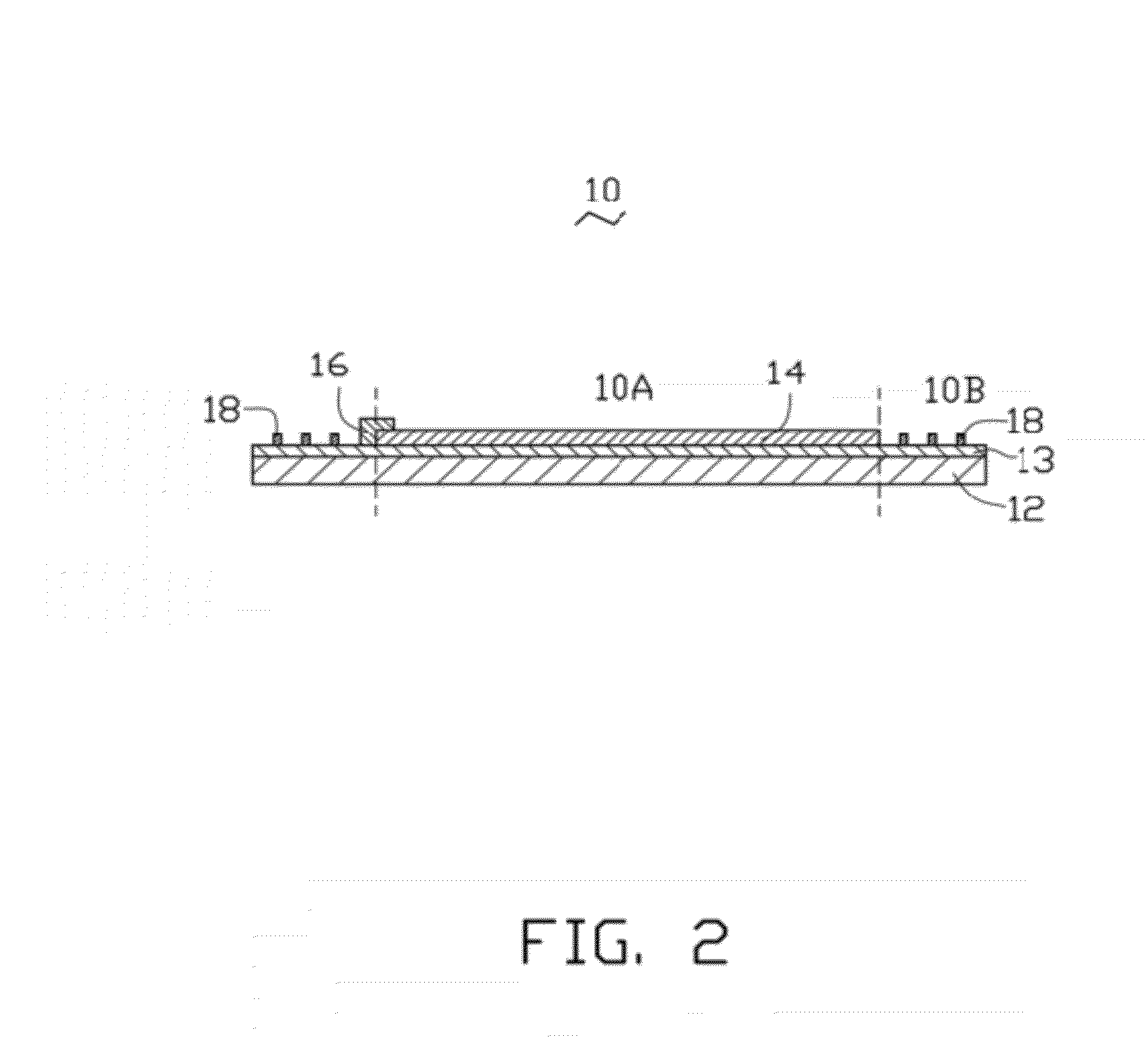
[0020]Referring to FIGS. 1 and 2, a touch panel 10 of one embodiment includes a substrate 12, a transparent conductive layer 14, at least one electrode 16, and a conductive trace 18.

[0021]The touch panel 10 defines two areas: a touch-view area 10A and a trace area 10B. The touch-view area 10A is typically a center area of the touch panel 10 which can be touched and viewed to realize the control function. The trace area 10B is usually a periphery area of the touch panel 10 which can be used to sup...


PUM

PropertyMeasurementUnit
lengthaaaaaaaaaa
lengthaaaaaaaaaa
thicknessaaaaaaaaaa

Abstract

The present disclosure relates to a touch panel. The touch panel includes a substrate having a surface, a transparent conductive layer, at least one electrode, and a conductive trace. The substrate defines a touch-view area and a trace area. The transparent conductive layer is located on the surface of the substrate and on only the touch-view area. The transparent conductive layer includes a carbon nanotube film. The at least one electrode is electrically connected with the transparent conductive layer. The conductive trace is located on only the trace area and electrically connected with the at least one electrode.

Description

CROSS-REFERENCE TO RELATED APPLICATIONS[0001]This application claims all benefits accruing under 35 U.S.C. §119 from Taiwan Patent Application No. 100120204, filed on Jun. 9, 2011, in the Taiwan Intellectual Property Office, the contents of which are hereby incorporated by reference. This application is related to applications entitled, “TOUCH PANEL”, filed ______ (Atty. Docket No. US39777); and “METHOD FOR MAKING TOUCH PANEL”, filed ______ (Atty. Docket No. US39779); and “METHOD FOR MAKING TOUCH PANEL”, filed ______ (Atty. Docket No. US39780); and “METHOD FOR MAKING TOUCH PANEL”, filed ______ (Atty. Docket No. US39781); and “TOUCH PANEL AND METHOD FOR MAKING THE SAME”, filed ______ (Atty. Docket No. US39782); and “METHOD FOR MAKING TOUCH PANEL”, filed ______ (Atty. Docket No. US39784); and “METHOD FOR MAKING TOUCH PANEL”, filed ______ (Atty. Docket No. US39785); and “PATTERNED CONDUCTIVE ELEMENT”, filed ______ (Atty. Docket No. US39786); and “METHOD FOR MAKING PATTERNED CONDUCTIVE ...

Claims


Application Information

Patent Timeline
Patent Type & Authority Applications(United States)
IPC IPC(8): G06F3/041
CPCG06F2203/04103G06F3/041
Inventor CHENG, JIA-SHYONGHUANG, PO-SHANSHIH, PO-SHENGHU, CHUN-YICHAO, CHIH-HANWU, JEAH-SHENG
Owner SHIH HUA TECH LTD
Features
  • R&D
  • Intellectual Property
  • Life Sciences
  • Materials
  • Tech Scout
  • Unparalleled Data Quality
  • Higher Quality Content
  • 60% Fewer Hallucinations
Learn More