Wavelength conversion member, light emitting device and image display device, and method for manufacturing wavelength conversion member

a technology of light emitting devices and wavelength conversion members, which is applied in the direction of organic semiconductor devices, lighting and heating devices, instruments, etc., can solve the problem of difficult to achieve sufficient emission efficiency, and achieve the effect of high emission efficiency

Inactive Publication Date: 2012-12-20
SHARP KK
View PDF10 Cites 90 Cited by
  • Summary
  • Abstract
  • Description
  • Claims
  • Application Information

AI Technical Summary

Benefits of technology

[0047]According to the present invention, it is possible to provide a wavelength conversion member having high emission efficiency and a light emitting device and an image display device including the same.

Problems solved by technology

However, when such a constitution as that of the light emitting device disclosed in the above Japanese Patent Laying-Open No. 2005-285800 is employed, it becomes difficult to realize sufficiently high emission efficiency due to concentration quenching.

Method used


Image

  • Wavelength conversion member, light emitting device and image display device, and method for manufacturing wavelength conversion member
  • Wavelength conversion member, light emitting device and image display device, and method for manufacturing wavelength conversion member
  • Wavelength conversion member, light emitting device and image display device, and method for manufacturing wavelength conversion member

Examples


embodiment 1

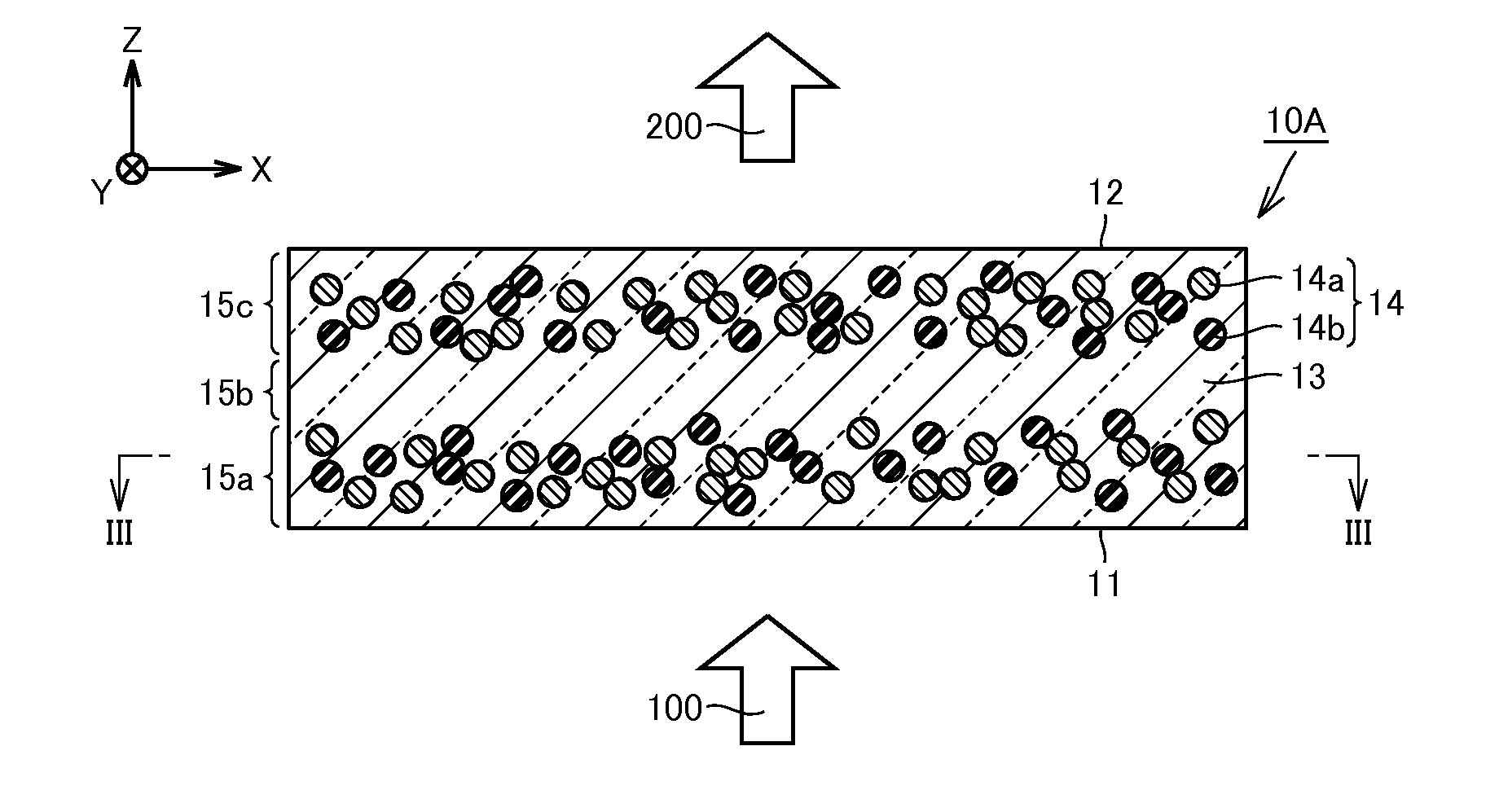
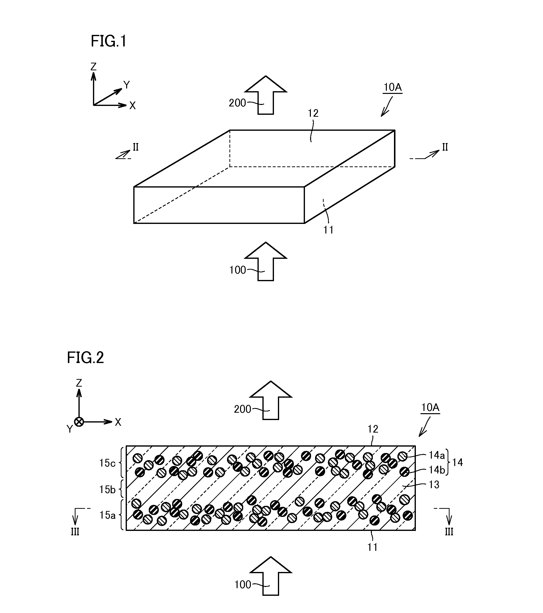
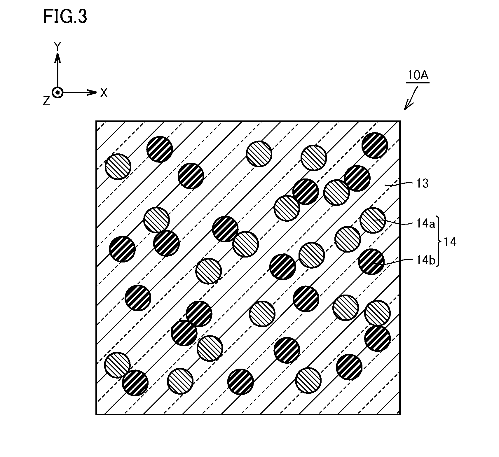
[0107]FIG. 1 is a schematic perspective view of a wavelength conversion member in Embodiment 1 of the present invention. FIG. 2 is a schematic section view of the wavelength conversion member in the present embodiment, cut along the XZ plane. FIG. 3 is a schematic section view of the wavelength conversion member in the present embodiment, cut along the XY plane. The section shown in FIG. 2 is a schematic section along the line II-II shown in FIG. 1. The section shown in FIG. 3 is a schematic section along the line III-III shown in FIG. 2. First, with reference to these FIG. 1 to FIG. 3, structure of the wavelength conversion member in the present embodiment will be described.

[0108]As shown in FIG. 1, a wavelength conversion member 10A in the present embodiment is formed from a member in the shape of a substantially rectangular parallelepiped having a predetermined thickness, and has a function of absorbing at least part of input light and outputting light having a wavelength that is...

embodiment 3

[0206]Here, also in wavelength conversion member 10D in the present embodiment, those having substantially equal particle sizes are used as semiconductor fine particle phosphors 14a, 14b, and semiconductor fine particle phosphors 14a, 14b are regularly arrayed in the form of hexagonal lattice in the XY plane of region 17a and in the XY plane of region 17c. Also in wavelength conversion member 10D constituted in this manner, it becomes possible to make difference between concentrations of semiconductor fine particle phosphors 14a, 14b in the Z axial direction and concentrations of semiconductor fine particle phosphors 14a, 14b in the XY in-plane direction large, and it is possible to greatly improve emission efficiency while suppressing reabsorption of light. A concrete method for manufacturing wavelength conversion member 10D is equivalent to the manufacturing method described in Embodiment 3 of the present invention, and description thereof will be omitted.

[0207]FIG. 13 is a schema...

embodiment 8

[0238]FIG. 18 is a schematic section view of a light emitting device in Embodiment 8 of the present invention. Next, referring to FIG. 18, structure of the light emitting device in the present embodiment will be described.

[0239]The light emitting device in the present embodiment has a structure combining a semiconductor light emitting diode element (hereinafter, also simply referred to as LED) as a light emitting element, and any one of wavelength conversion members 10A to 10G of Embodiments 1 to 7 of the present invention as described above. That is, the light emitting device in the present embodiment has a wavelength conversion member having specific anisotropy in dispersion concentrations of semiconductor fine particle phosphors as described above. Here, description for the anisotropy in dispersion concentration is omitted because it is redundant. In a light emitting device 30 shown in FIG. 18, the one including wavelength conversion member 10A in Embodiment 1 of the present inve...


PUM


Abstract

Disclosed is a wavelength conversion member that is provided with: a light transmissive member including a light input plane into which excitation light is inputted, and a light output plane from which wavelength converted light is outputted; and a semiconductor fine particle phosphor, which is dispersed in the light transmissive member, and which absorbs the excitation light, converts the wavelength, and emits light. The dispersion concentration of the semiconductor fine particle phosphor in the direction parallel to the light traveling direction, i.e., the direction connecting the light input plane and the light output plane, is lower than the dispersion concentration of the semiconductor fine particle phosphor in the direction orthogonal to the light traveling direction.

Description

REFERENCE TO RELATED APPLICATIONS[0001]This application is a national stage application under 35 USC 371 of International Application No. PCT / JP2011 / 054270, filed Feb. 25, 2011, which claims priority from Japanese Patent Application Nos. 2010-046147, filed Mar. 3, 2010, and 2011-030333, filed Feb. 16, 2011, the entire contents of which are incorporated herein by reference.FIELD OF THE INVENTION[0002]The present invention relates to a wavelength conversion member that converts wavelength of at least part of input light and outputs the resultant light, and a light emitting device and an image display device having the same, and more specifically, to a wavelength conversion member containing a semiconductor fine particle phosphor dispersed in a light transmissive member, and a light emitting device and an image display device including the same. Also, the present invention relates to a method for manufacturing the wavelength conversion member.BACKGROUND OF THE INVENTION[0003]Recently, ...

Claims


Application Information

Patent Timeline
Patent Type & Authority Applications(United States)
IPC IPC(8): F21V9/16
CPCH01L2924/181H01L2224/48091H01L2224/73265H01L2924/00012H01L2924/00014G02F1/133621H01L27/322H01L33/504H01L33/505H01L2251/5369G02F2001/133614G02F2202/102G02F1/133614H10K59/38H10K2102/331
Inventor KINOMOTO, JUNICHIRYOWA, TATSUYA
Owner SHARP KK
Why Eureka
Try Eureka