

Dc/dc convertor power module package incorporating a stacked controller and construction methodology
a technology of power module and stacked controller, which is applied in the direction of resistors, basic electric elements, solid-state devices, etc., can solve the problems of increasing fabrication costs, increasing the failure rate of the packages produced, and increasing the problem of large surface area
- Summary
- Abstract
- Description
- Claims
- Application Information
AI Technical Summary
Benefits of technology
Problems solved by technology
Method used
Image

Examples
Embodiment Construction
[0021]Reference is made to particular embodiments of the invention. Examples of which are illustrated in the accompanying drawings. While the invention will be described in conjunction with particular embodiments, it will be understood that it is not intended to limit the invention to the described embodiments. To contrary, the disclosure is intended to extend to cover alternatives, modifications, and equivalents as may be included within the spirit and scope of the invention as defined by the appended claims.
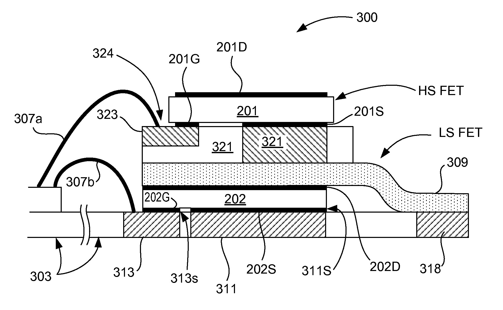
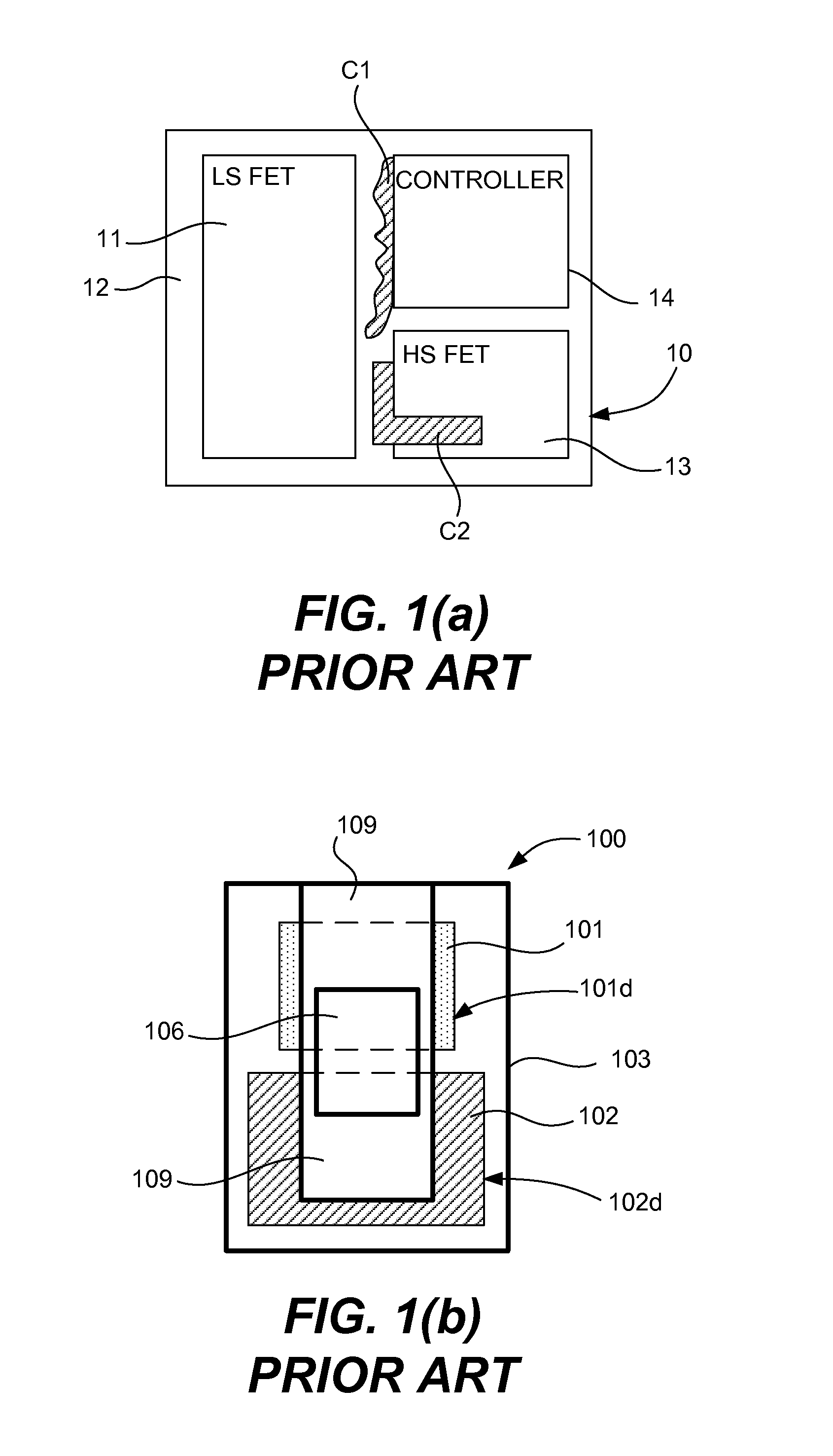
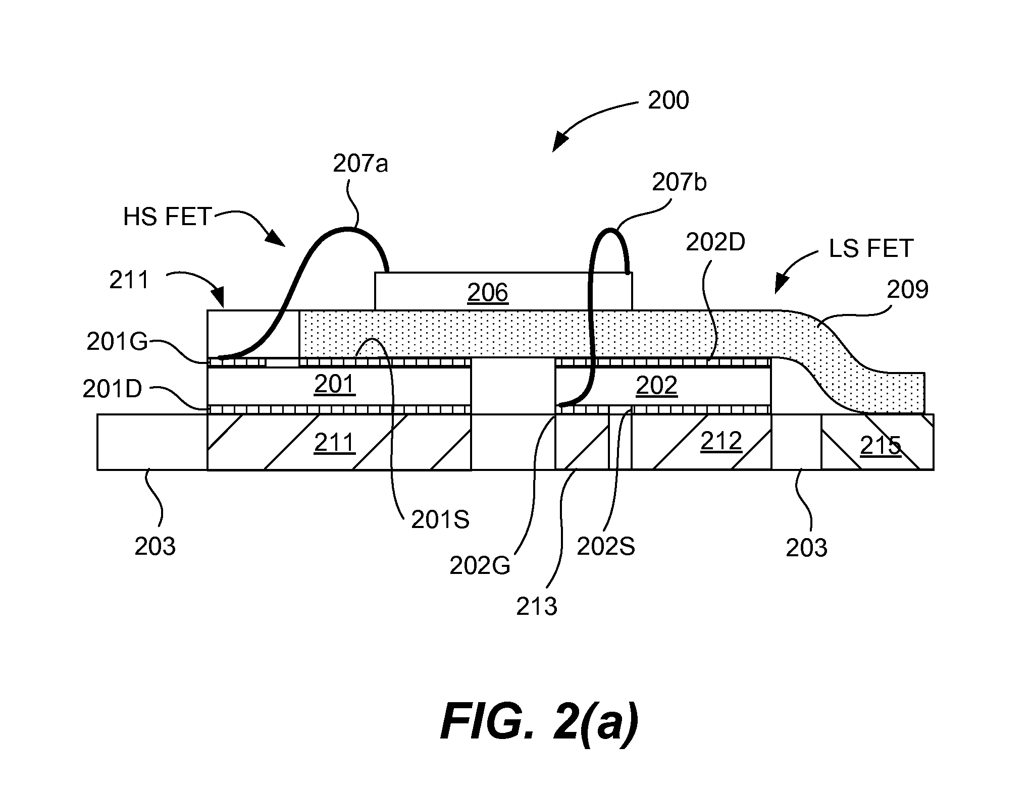
[0022]Aspects of the invention pertain to novel power converter modules or devices used in power level shifting applications and the methods of fabricating and packaging such devices. Such power converters are used in DC-DC voltage level shifting devices. For example in DC-DC step down level shifters and the like. In one example, a synchronous buck topology can be used in power converter modules used, for example, in a DC-DC power level shifter. Aims of the inventive technologi...
PUM
 Abstract
Description
Claims
Application Information