Display device and drive method therefor

a technology of a display device and a drive method, which is applied in the field of display devices, can solve the problems of increasing manufacturing costs and complex circuits, and achieve the effects of reducing the number of output buffers provided in reducing the circuit size of the power control circuit, and reducing the number of elements in each pixel circui

Active Publication Date: 2013-01-24
SHARP KK
View PDF3 Cites 10 Cited by
  • Summary
  • Abstract
  • Description
  • Claims
  • Application Information

AI Technical Summary

Benefits of technology

[0027]According to the first or fourteenth aspect of the present invention, by applying an initialization potential to the common power line(s) using the power control circuit, the initialization potential can be provided to the pixel circuits from the power lines. Accordingly, the number of elements in each pixel circuit can be reduced. In addition, the power control circuit drives the common power line(s), each connected to two or more power lines. Therefore, compared to the case of individually driving the power lines, the number of output buffers provided in the power control circuit is reduced, making it possible to reduce the circuit size of the power control circuit.
[0028]According to the second aspect of the present invention, initialized pixel circuits are selected on a row basis, and the selected pixel circuits perform threshold detection, writing, and light emission in turn. Accordingly, threshold voltages of the driving transistors are compensated for and then a screen can be displayed.
[0029]According to the third aspect of the present invention, by controlling the light emission control transistor to an on state by applying an initialization potential to the power line, the initialization potential can be applied to the other conduction terminal of the driving transistor.
[0030]According to the fourth aspect of the present invention, by controlling the light emission control transistor to an off state upon completion of initialization and controlling the light emission control transistor to an on state upon threshold detection, the pixel circuit can be allowed to turn off during a period from the initialization to the threshold detection. In addition, upon threshold detection, by supplying a current from the power line, a threshold of the driving transistor can be detected.
[0031]According to the fifth aspect of the present invention, by controlling the light emission control transistors to an on state for a fixed period of time upon light emission, the lengths of the light emission periods of the pixel circuits are made the same, making it possible to suppress variations in luminance. In addition, since the pixel circuits turn off during periods other than the light emission period, moving image performance can be improved as in the case of performing black insertion.
[0032]According to the sixth aspect of the present invention, by controlling the reference potential application transistor to an on state upon threshold detection, a reference potential is applied to the control terminal of the driving transistor from the reference potential line, making it possible to detect a threshold of the driving transistor. In addition, since the reference potential application transistor can be controlled to an on state at relatively flexible timing, a threshold detection period can be freely set.

Problems solved by technology

In general, the larger the number of wiring lines (particularly, control lines) connected to a pixel circuit, the more complex the circuit becomes, increasing manufacturing cost.

Method used


Image

  • Display device and drive method therefor
  • Display device and drive method therefor
  • Display device and drive method therefor

Examples


first embodiment

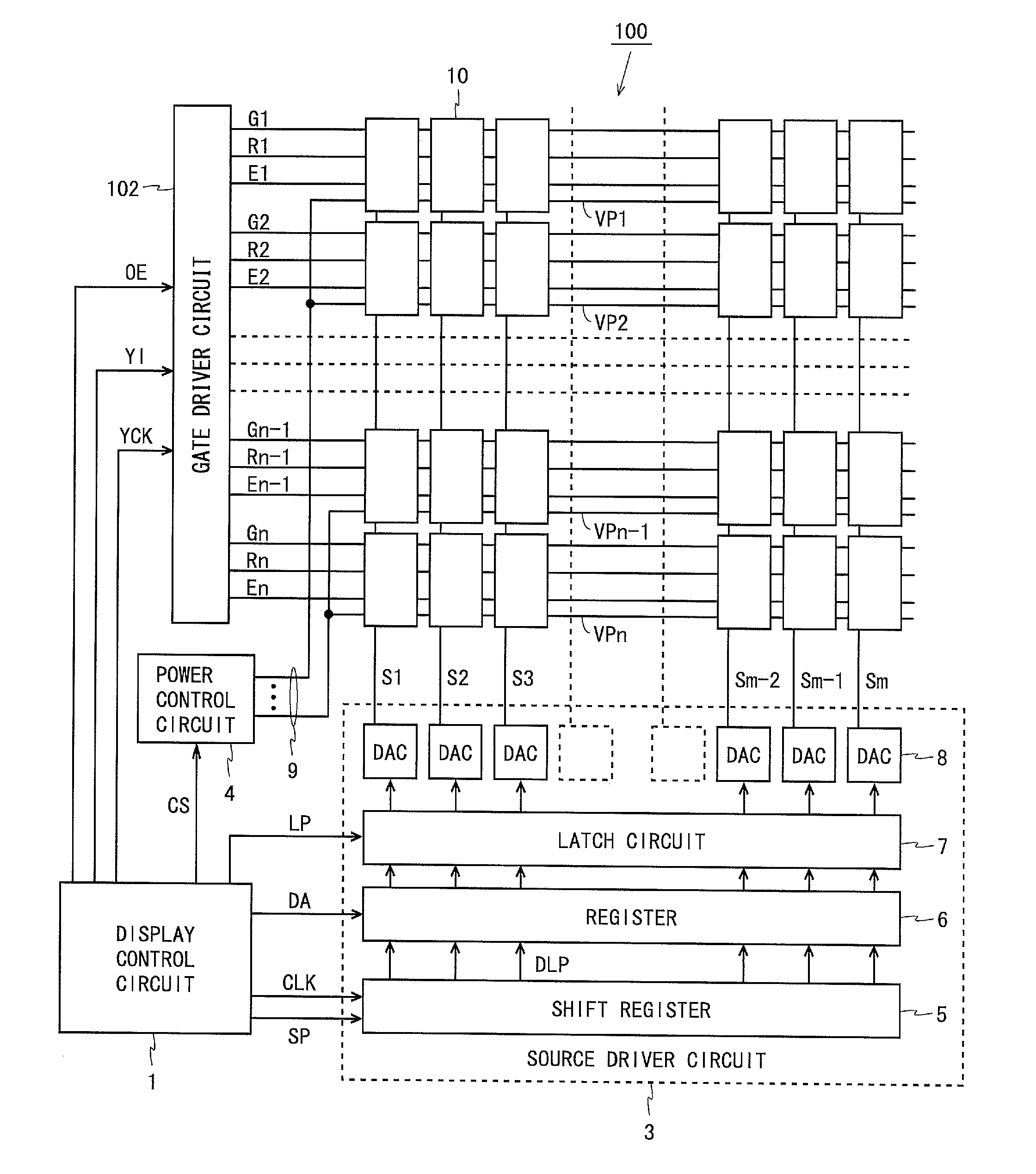
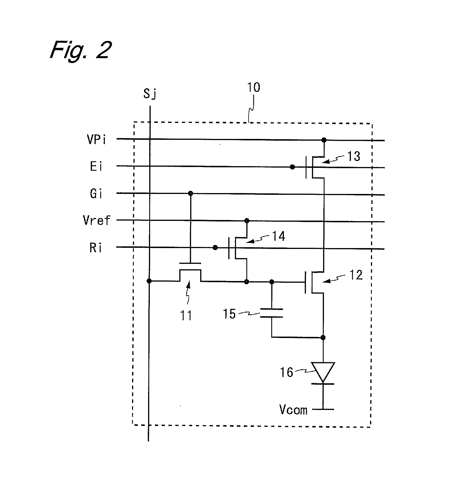
[0059]FIG. 1 is a block diagram showing a configuration of a display device according to a first embodiment of the present invention. A display device 100 shown in FIG. 1 is an organic EL display including a display control circuit 1, a gate driver circuit 102, a source driver circuit 3, a power control circuit 4, and (m×n) pixel circuits 10. In the following, m and n are integers not smaller than 2, i is an integer between 1 and n inclusive, and j is an integer between 1 and m inclusive.

[0060]In the display device 100, n control lines Gi parallel to one another and m data lines Sj parallel to one another and intersecting with the control lines Gi perpendicularly are provided. The (m×n) pixel circuits 10 are arranged two-dimensionally at respective intersections of the control lines Gi and the data lines Sj. In addition, n control lines Ri, n control lines Ei, and n power lines VPi are provided parallel to the control lines Gi. Furthermore, to connect the power control circuit 4 to ...

second embodiment

[0106]FIG. 12 is a block diagram showing a configuration of a display device according to a second embodiment of the present invention. A display device 200 shown in FIG. 12 includes a gate driver circuit 202 and pixel circuits 20 instead of the gate driver circuit 102 and the pixel circuits 10. Of the components of the present embodiment, the same components as those of the first embodiment are denoted by the same reference characters and description thereof is omitted.

[0107]In the display device 200, (n+1) control lines G0 to Gn are provided and n control lines Ei and n power lines VPi are provided parallel to the (n+1) control lines G0 to Gn. The control lines G0 to Gn and Ei are connected to the gate driver circuit 202. Though not shown, pixel circuits in an i-th row are also connected to a control line Gi-1 in a previous row. The display device 200 does not include control lines Ri or wiring lines for a reference potential Vref.

[0108]FIG. 13 is a circuit diagram of the pixel ci...

third embodiment

[0115]FIG. 15 is a block diagram showing a configuration of a display device according to a third embodiment of the present invention. A display device 300 shown in FIG. 15 includes a gate driver circuit 302 and pixel circuits 30 instead of the gate driver circuit 102 and the pixel circuits 10. Of the components of the present embodiment, the same components as those of the first embodiment are denoted by the same reference characters and description thereof is omitted.

[0116]In the display device 300, n control lines Ei and n power lines VPi are provided parallel to n control lines Gi. The control lines Gi and Ei are connected to the gate driver circuit 302. The display device 300 does not include control lines Ri or wiring lines for a reference potential Vref.

[0117]FIG. 16 is a circuit diagram of the pixel circuit 30. As shown in FIG. 16, the pixel circuit 30 includes TFTs 31 to 33, a capacitor 35, and an organic EL element 36. The pixel circuit 30 is connected to the control lines...


PUM


Abstract

A display device 100 includes a plurality of pixel circuits 10 arranged two-dimensionally; a plurality of power lines VPi provided for respective rows of the pixel circuits 10; p common power lines 9, each connected to two or more power lines VPi; and a power control circuit 4. Each pixel circuit 10 includes an organic EL element, a plurality of TFTs, and a capacitor and receives an initialization potential from a corresponding power line VPi. The power control circuit 4applies a power supply potential and the initialization potential to the p common power lines 9 in a switching manner. Accordingly, a display device is provided that has a configuration in which an initialization potential is provided to pixel circuits from power lines and that has a power control circuit small in circuit size.

Description

TECHNICAL FIELD[0001]The present invention relates to a display device and, more particularly to a display device using current-driven elements such as an organic EL display, and a drive method therefor.BACKGROUND ART[0002]As a thin, high image quality, and low power consumption display device, an organic EL (Electro Luminescence) display is known. The organic EL display includes a plurality of pixel circuits including an organic EL element and a driving transistor. When providing display on the organic EL display, there is a need to compensate for variations in the threshold voltage of the driving transistors and an increase in resistance caused by deterioration over time of the organic EL elements.[0003]Various types of pixel circuits that perform compensation operation are conventionally known. Patent Document 1 describes a pixel circuit 80 shown in FIG. 18. The pixel circuit 80 includes TFTs (Thin Film Transistors) 81 to 85, a capacitor 86, and an organic EL element 87. When wri...

Claims


Application Information

Patent Timeline
Patent Type & Authority Applications(United States)
IPC IPC(8): G06F3/038
CPCG09G3/3225G09G3/3275G09G2330/028G09G2300/0819G09G2300/0861G09G2300/0814
Inventor KISHI, NORITAKA
Owner SHARP KK
Why Eureka
Try Eureka