Supercharge Your Innovation With Domain-Expert AI Agents!

Light emitting chip package and method for making same

a technology of light-emitting chips and packages, which is applied in the direction of electrical equipment, semiconductor/solid-state device manufacturing, and semiconductor devices. it can solve the problems of inability to avoid gaps between the interior sidewalls of through holes and electrode portions, and undetectable leakage of adhesive during the process

Inactive Publication Date: 2013-01-31
HON HAI PRECISION IND CO LTD
View PDF4 Cites 14 Cited by
  • Summary
  • Abstract
  • Description
  • Claims
  • Application Information

AI Technical Summary

Benefits of technology

The present patent relates to a light emitting chip package and a method for making the same. The technical effect of the patent is to provide an LED package that can effectively avoid adhesive leak during the packaging process. The patent describes various embodiments of the LED package structure and method for making the same, including a substrate, an etch stop layer, an insulation layer, an electric conductive layer, a light emitting chip, an encapsulation, metallic thermal conductors, and electrical conductors. The patent also discusses the formation of a step hole and recesses in the substrate, as well as the use of an etch stop layer. Overall, the patent aims to provide a reliable LED package with improved reliability and performance.

Problems solved by technology

However, it is hard to avoid gaps remained between interior sidewalls of the through holes and the electrode portions.
As such, leak of adhesive undesirably occurs during the injection of liquid encapsulating materials.

Method used


Image

  • Light emitting chip package and method for making same
  • Light emitting chip package and method for making same
  • Light emitting chip package and method for making same

Examples


Embodiment Construction

[0015]Reference will now be made to the drawings to describe the present light emitting chip package structure and method for making the same, in detail.

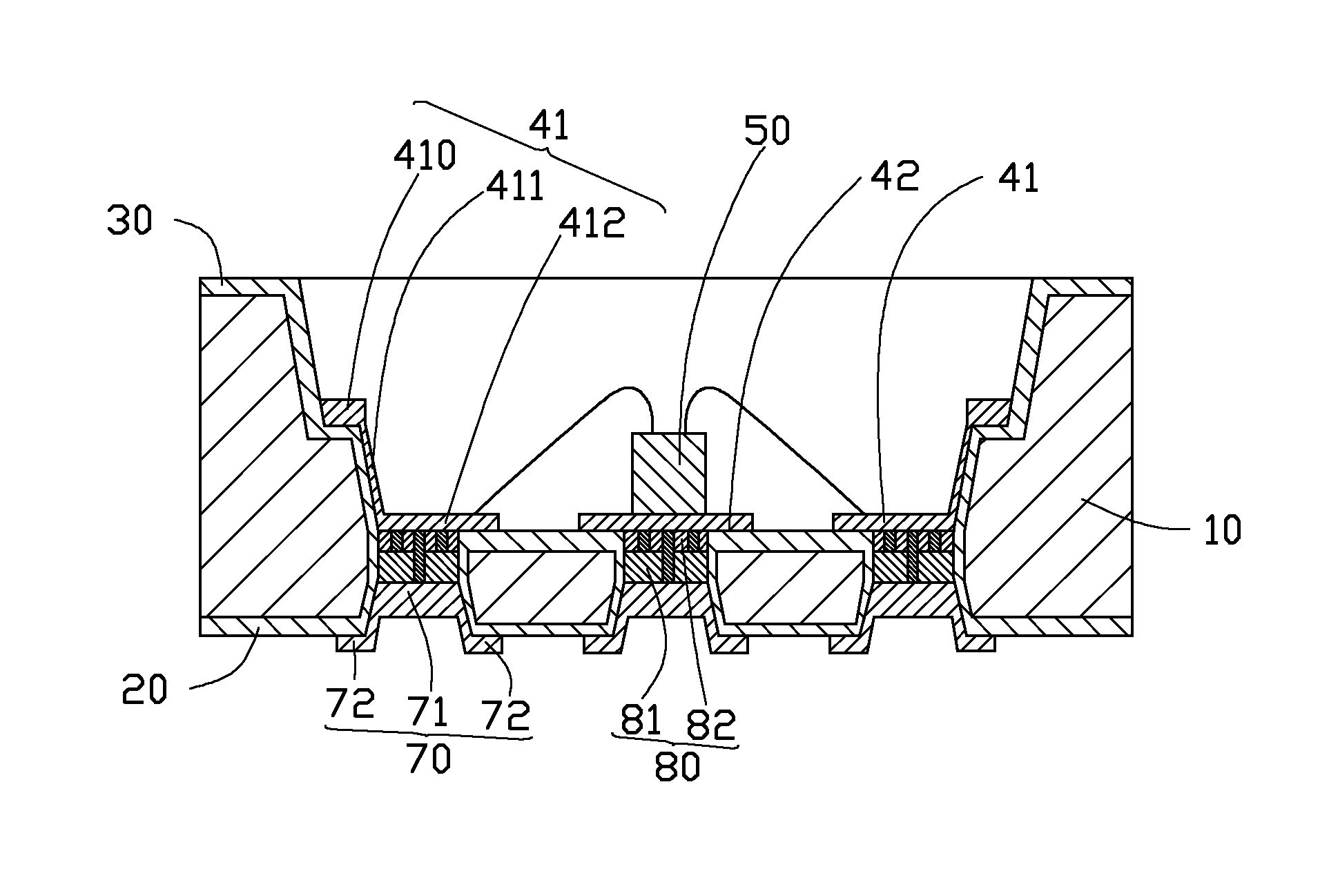
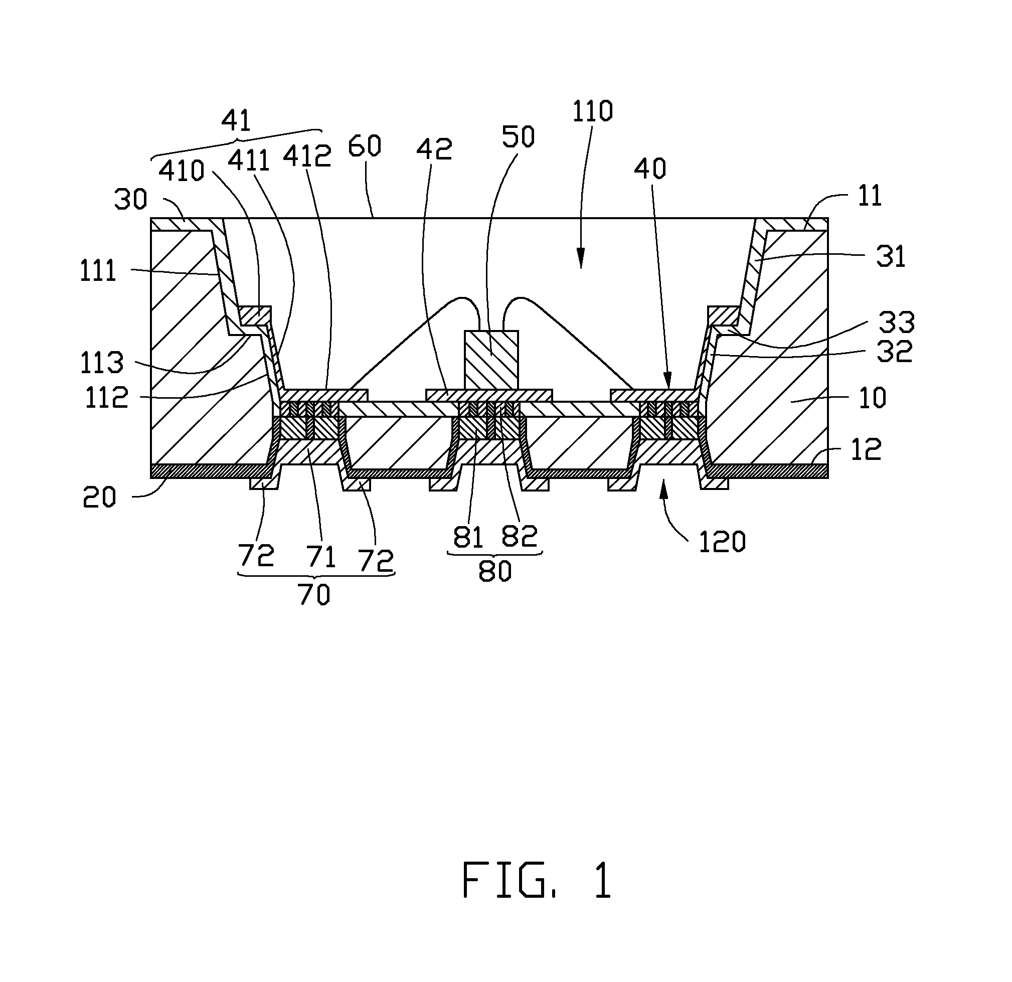
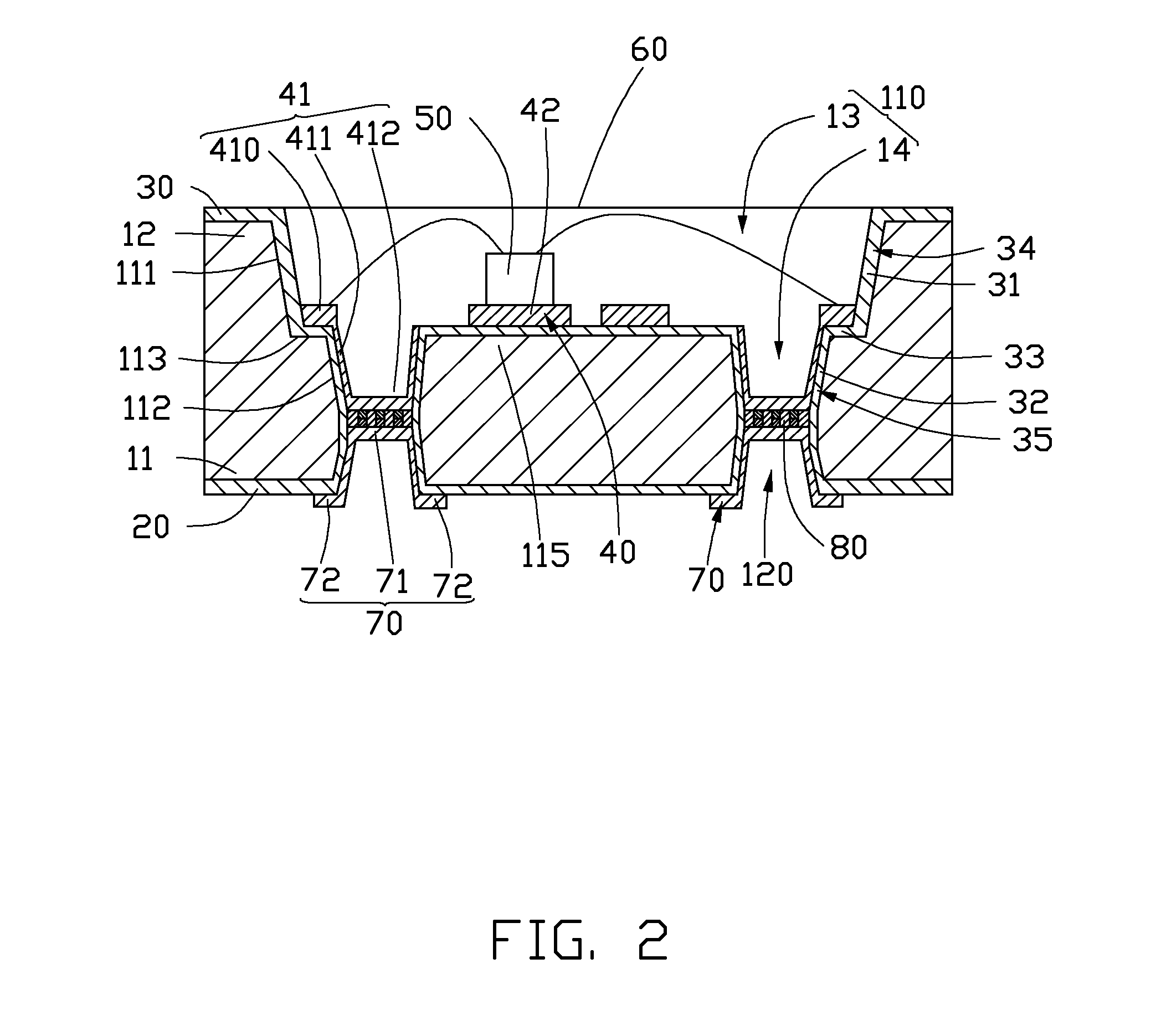
[0016]Referring to FIG. 1, a light emitting chip package according to a first embodiment includes a substrate 10, an etch stop layer 20, an insulation layer 30, an electric conductive layer 40, a light emitting chip 50, an encapsulation 60, a plurality of metallic thermal conductors 70 and a plurality of electrical conductors 80.

[0017]The substrate 10 includes a top surface 11 and a bottom surface 12 opposite to the top surface 11. The substrate 10 can be made of electrical conductive materials, for example cooper. The substrate 10 can also be made of insulated materials such as silicon (Si), gallium arsenide (GaAs), zinc oxide (ZnO), indium phosphide (InP) and combination thereof.

[0018]A step hole 110 is formed in the top surface 11. The step hole 110 includes two side surfaces symmetric to each other. Each side surface of the step...


PUM


Abstract

A light emitting chip package includes a substrate, an insulation layer, a patterned electric conductive layer, a light emitting chip, an encapsulation, a plurality of thermal conductors and electrical conductors. The insulation layer is formed on a top surface of the substrate. The patterned electric conductive layer partially covers the insulation layer. The light emitting chip is arranged on the electric conductive layer. The encapsulation covers the light emitting chip and the electric conductive layer. The plurality of thermal conductors is formed at a bottom surface side of the substrate. The plurality of electrical conductors penetrates the insulation layer and connects the conductive layer with the thermal conductor. The plurality of electrical conductors is isolated from each other.

Description

BACKGROUND[0001]1. Technical Field[0002]The present disclosure generally relates to light emitting chip packages, and method for making the same.[0003]2. Description of Related Art[0004]In recent years, due to excellent light quality and high luminous efficiency, light emitting diodes (LEDs) have increasingly been used as substitutes for incandescent bulbs, compact fluorescent lamps and fluorescent tubes as light sources of illumination devices.[0005]However, since the LED radiates large amounts of heat when current is applied thereto, an LED must efficiently radiate large amounts of heat generated upon operation thereof, to achieve high reliability.[0006]During package process of LEDs, a substrate for supporting a LED chip is generally configured with a plurality of through holes adapted to have electrode inserted therein. However, it is hard to avoid gaps remained between interior sidewalls of the through holes and the electrode portions. As such, leak of adhesive undesirably occu...

Claims


Application Information

Patent Timeline
IPC IPC(8): H01L33/52H01L33/62
CPCH01L33/486H01L33/642H01L2933/005H01L33/62H01L2224/48091H01L33/52H01L2924/00014
Inventor TSANG, JIAN-SHIHN
Owner HON HAI PRECISION IND CO LTD
Features
  • R&D
  • Intellectual Property
  • Life Sciences
  • Materials
  • Tech Scout
  • Unparalleled Data Quality
  • Higher Quality Content
  • 60% Fewer Hallucinations
Learn More