Semiconductor device and manufacturing method thereof

a technology of semiconductors and semiconductors, applied in the field of semiconductor devices, can solve problems such as deteriorating device performance, and achieve the effect of reducing or eliminating pmos performance and reducing stacking faults

Active Publication Date: 2013-02-14
SEMICONDUCTOR MANUFACTURING INTERNATIONAL (BEIJING) CORP
View PDF1 Cites 300 Cited by
  • Summary
  • Abstract
  • Description
  • Claims
  • Application Information

AI Technical Summary

Benefits of technology

[0029]An advantage of the present invention is that stacking faults can be eliminated or reduced while high content of Ge can be achieved in embedded SiGe source/drain regions, thus improving the PMOS p...

Problems solved by technology

% (atomic percent)) may cause substantial stacking faults to occur on...

Method used


Image

  • Semiconductor device and manufacturing method thereof
  • Semiconductor device and manufacturing method thereof
  • Semiconductor device and manufacturing method thereof

Examples


Embodiment Construction

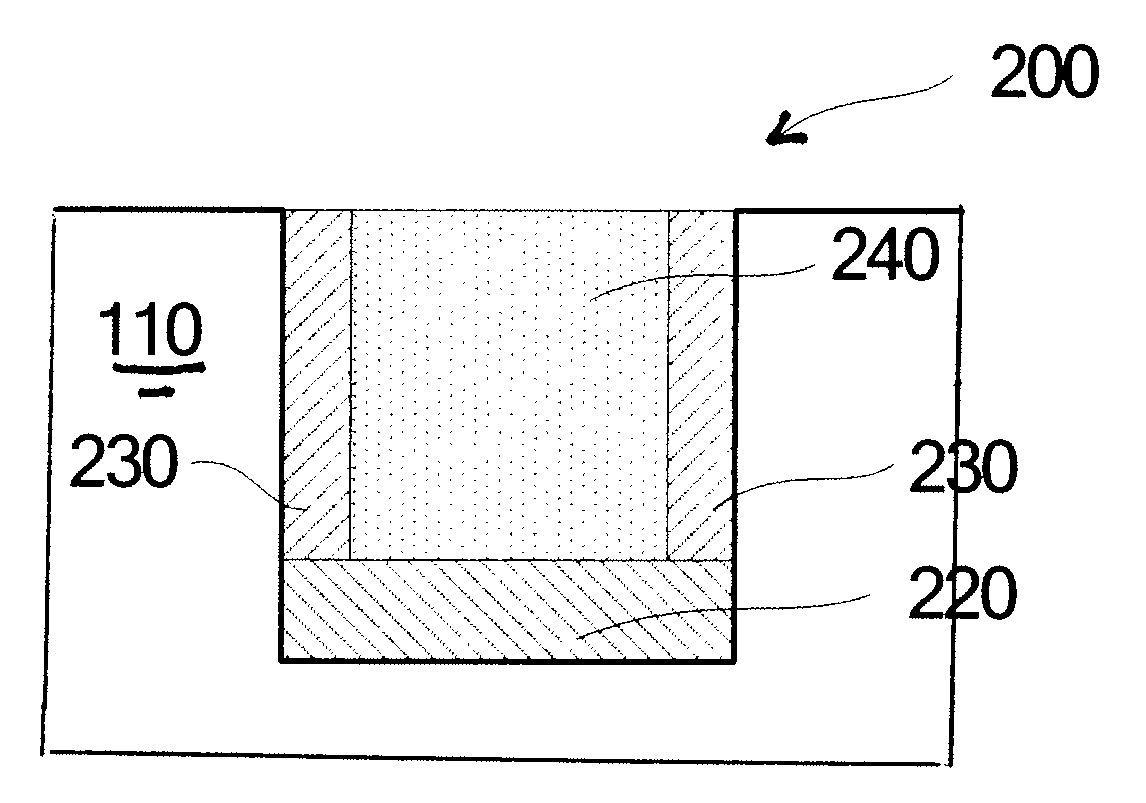
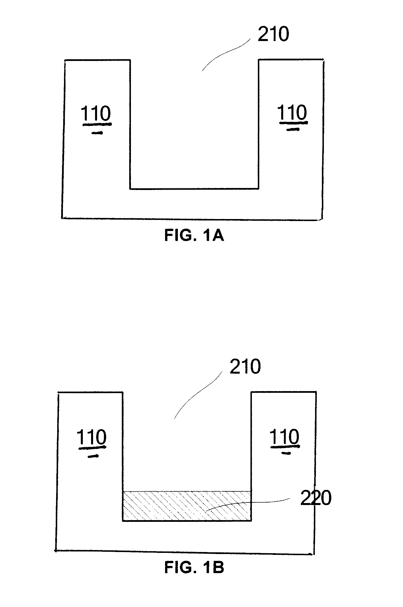
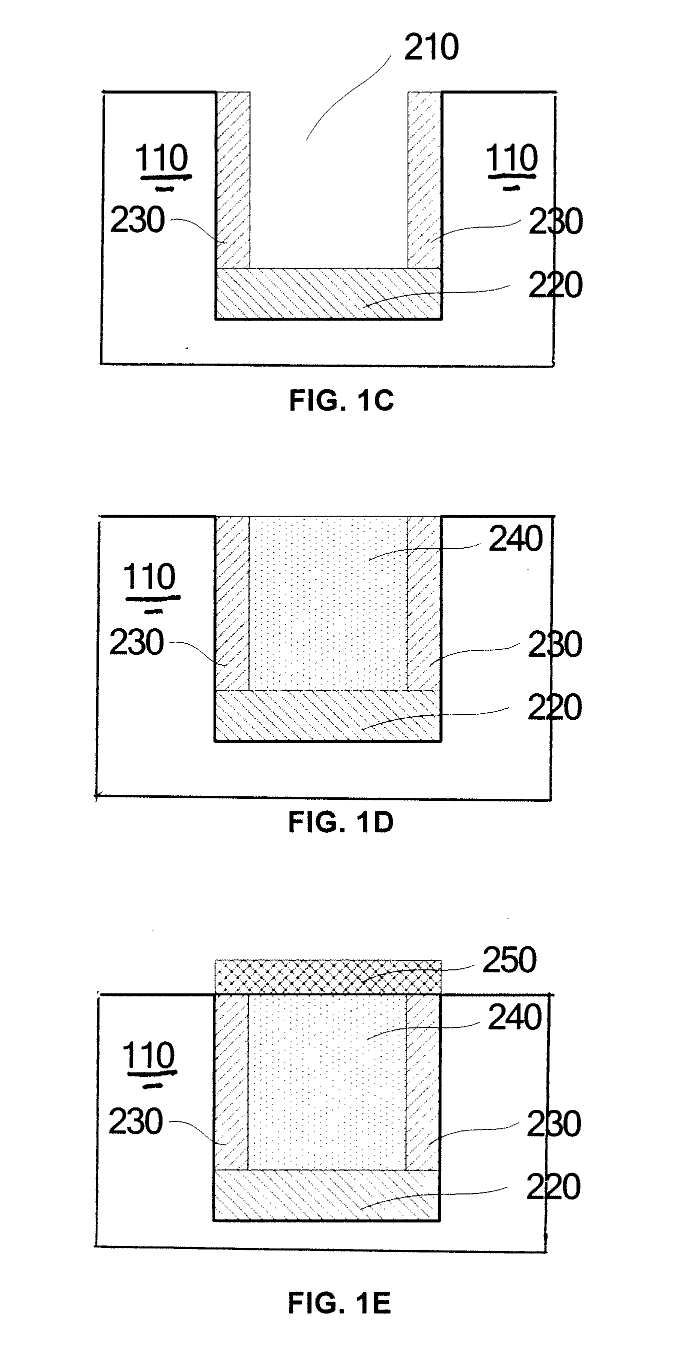
[0035]Various exemplary embodiments of the present invention will now be described in detail with reference to the drawings. It is understood that the relative arrangement of the components and steps, the numerical expressions and numerical values set forth in these embodiments do not limit the scope of the present invention unless it is specifically stated otherwise.

[0036]At the same time, is also understood that for the simplicity of description, each part in these figures may not be drawn to scale.

[0037]The following description of at least one exemplary embodiment is merely illustrative in nature and is in no way intended to limit the invention, its application or uses.

[0038]Techniques, methods and apparatus as known by one of ordinary skill in the relevant art may not be discussed in detail but are intended to be part of the specification where appropriate.

[0039]In all of the examples illustrated and discussed herein, any specific values should be interpreted to be illustrative...


PUM


Abstract

This invention relates to a semiconductor device and a manufacturing method thereof for reducing stacking faults caused by high content of Ge in an embedded SiGe structure. The semiconductor device comprises a Si substrate with a recess formed therein. A first SiGe layer having a Ge content gradually increased from bottom to top is formed on the recess bottom, a SiGe seed layer is formed on sidewalls of the recess and a second SiGe layer having a constant content of Ge is formed on the first SiGe layer. The thickness of the first SiGe layer is less than the depth of the recess. The Ge content in the SiGe seed layer is less than the Ge content in the second SiGe layer and the Ge content at the upper surface of the first SiGe layer is less than or equal to the Ge content in the second SiGe layer.

Description

CROSS-REFERENCE TO RELATED APPLICATIONS[0001]This application claims priority to Chinese Patent Application No. 201110227479.9, filed on Aug. 10, 2011 and entitled “Semiconductor Device and Manufacturing Method thereof,” which is incorporated herein in its entirety by reference.BACKGROUND OF THE INVENTION[0002]1. Field of the Invention[0003]The present invention relates to the semiconductor field, and specifically, to a semiconductor device and a manufacturing method therefor.[0004]2. Description of the Related Art[0005]With the continuous development of semiconductor techniques, carrier mobility enhancement techniques have been widely investigated and utilized. Carrier mobility improvement in a channel region may increase the driving current of a MOS device, thus improving device performance.[0006]One effective mechanism for improving carrier mobility is to produce stress in a channel region. To this end, embedded SiGe techniques have been widely applied to improve the performance ...

Claims


Application Information

Patent Timeline
IPC IPC(8): H01L29/165H01L21/20
CPCH01L21/02381H01L21/0243H01L21/0245H01L21/0251H01L29/165H01L21/0262H01L29/66636H01L29/7848H01L21/02532
Inventor HONG, ZHONGSHANTU, HUOJIN
Owner SEMICONDUCTOR MANUFACTURING INTERNATIONAL (BEIJING) CORP
Why Eureka
Try Eureka