Optical semiconductor device comprising a multiple quantum well structure

Inactive Publication Date: 2005-02-01
OSRAM OLED
View PDF19 Cites 180 Cited by
  • Summary
  • Abstract
  • Description
  • Claims
  • Application Information

AI Technical Summary

Benefits of technology

It is an advantage of the present invention to improve the optical semiconductor device set out above.
The present invention achieves this and other advantages through an optical semiconductor device with a multiple quantum well structure, comprising: at least one combination of alternating well layers and barrier layersboth further comprising various semiconductor layers, said well layers further comprising a first composition based on a nitride semiconductor material with a first electron energy, said barrier layers further comprising a second composition of a nitride semiconductor material with electron energy which is higher in comparison with the first electron energy, and a radiation-active quantum well layer, layered in direction of growth for which the well layers and barrier layers form a superlattice.
The invention provides a multiple quatum well structure with well layers and barrier layers comprising various types of semiconductor layers which are layered alternatively one on top of the other. The well layers are thin layers of a first composition based on a nitride semiconductor material with a first electron energy. The barrier layers are layers which are thicker in comparion to the well layers, are of a second composition of a nitride semiconductor material and are with electron energy which is higher in comparison with the first electron energy. Acting as the radiation-active quatum well, seen in the direction of growth, is firstly one of the last quatum well layers or the last quatum well layer. The

Problems solved by technology

However, these quantum wells lead to a considerable increase in the forward voltage.
However, this adversely effects the cry

Method used


Image

  • Optical semiconductor device comprising a multiple quantum well structure
  • Optical semiconductor device comprising a multiple quantum well structure
  • Optical semiconductor device comprising a multiple quantum well structure

Examples


Example

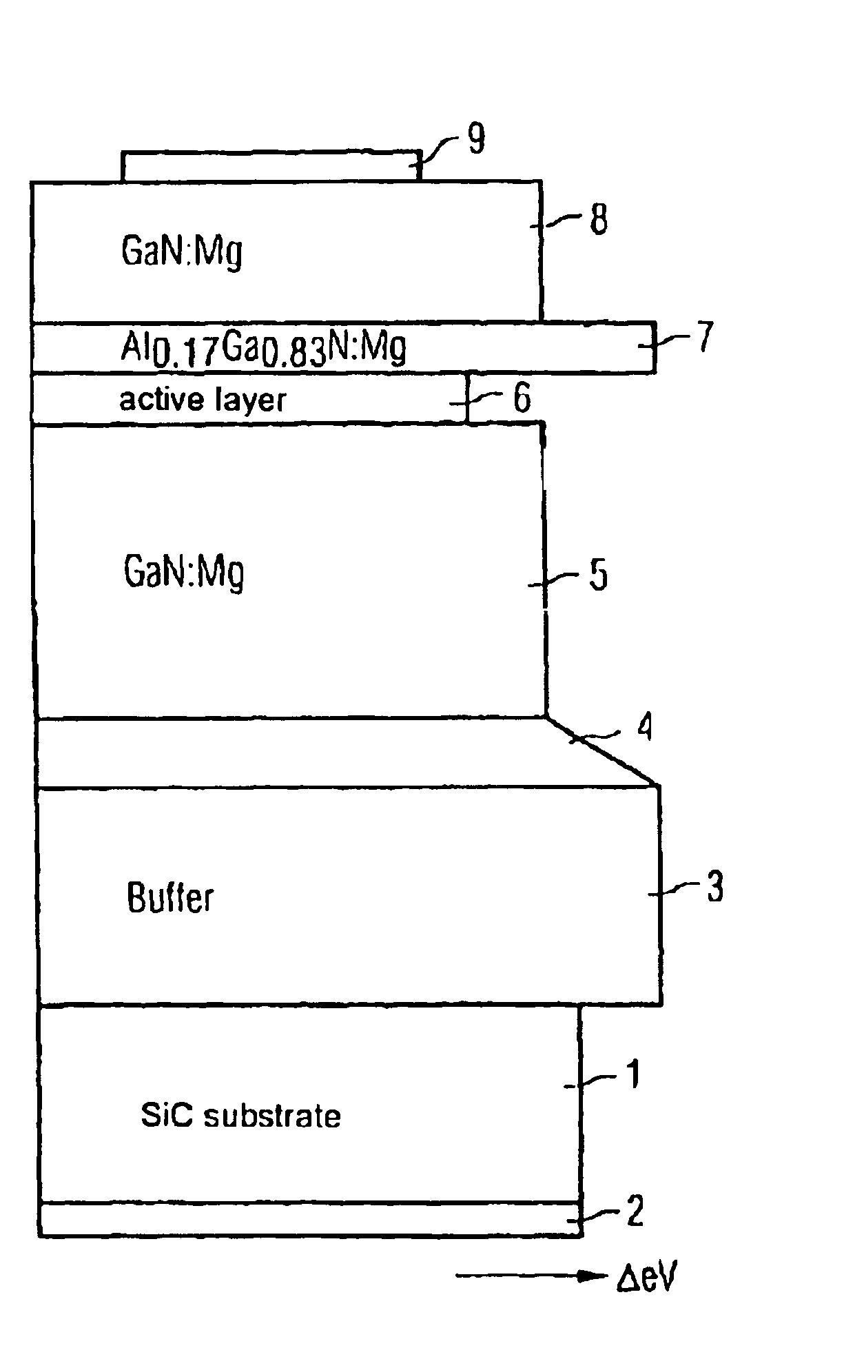
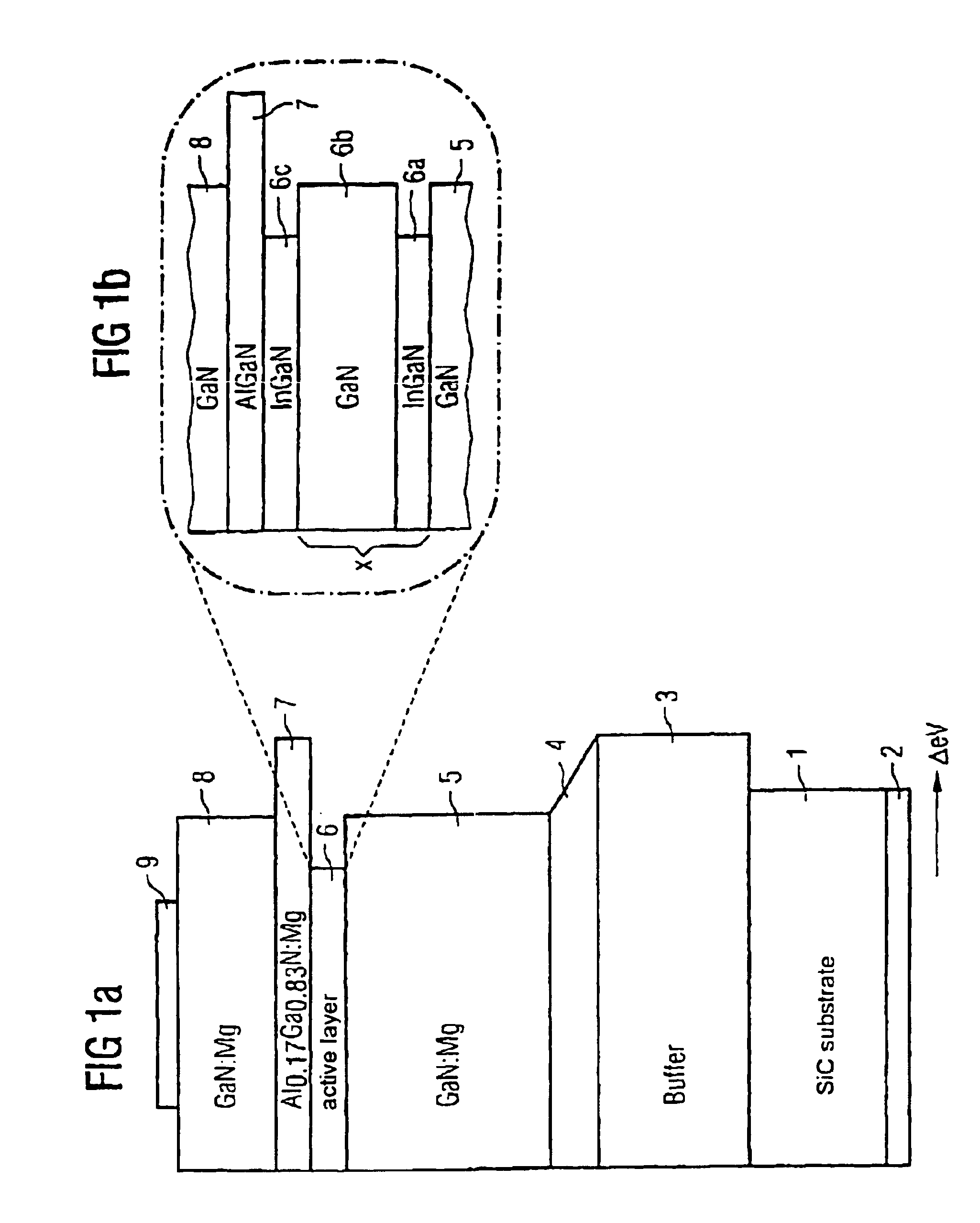
According to FIG. 1a, initially a buffer layer 3 of aluminum-gallium-nitride (AlGaN) is formed on a substrate 1 of silicon carbide (SiC), to which a first contact electrode 2 is connected. This is followed by a further layer 4 of aluminum-gallium-nitride. A further buffer layer 5 of silicon-doped gallium nitride is arranged over the layer 4. The quantum well structure 6a, 6b, still to be discussed in more detail, is arranged over buffer layer 5. Quantum well structure 6a and 6b are followed by the actual active layer 6c. Arranged over the active layer 6 is a further layer 7 of aluminum-gallium-nitride, which serves as an electron barrier. This layer 7 is preferably doped with magnesium. A further GaN layer, not designated, may be arranged between the layers 6 and 7. A gallium-nitride layer 8, on which a second contact electrode 9 of the device is provided, is arranged over the layer 7.

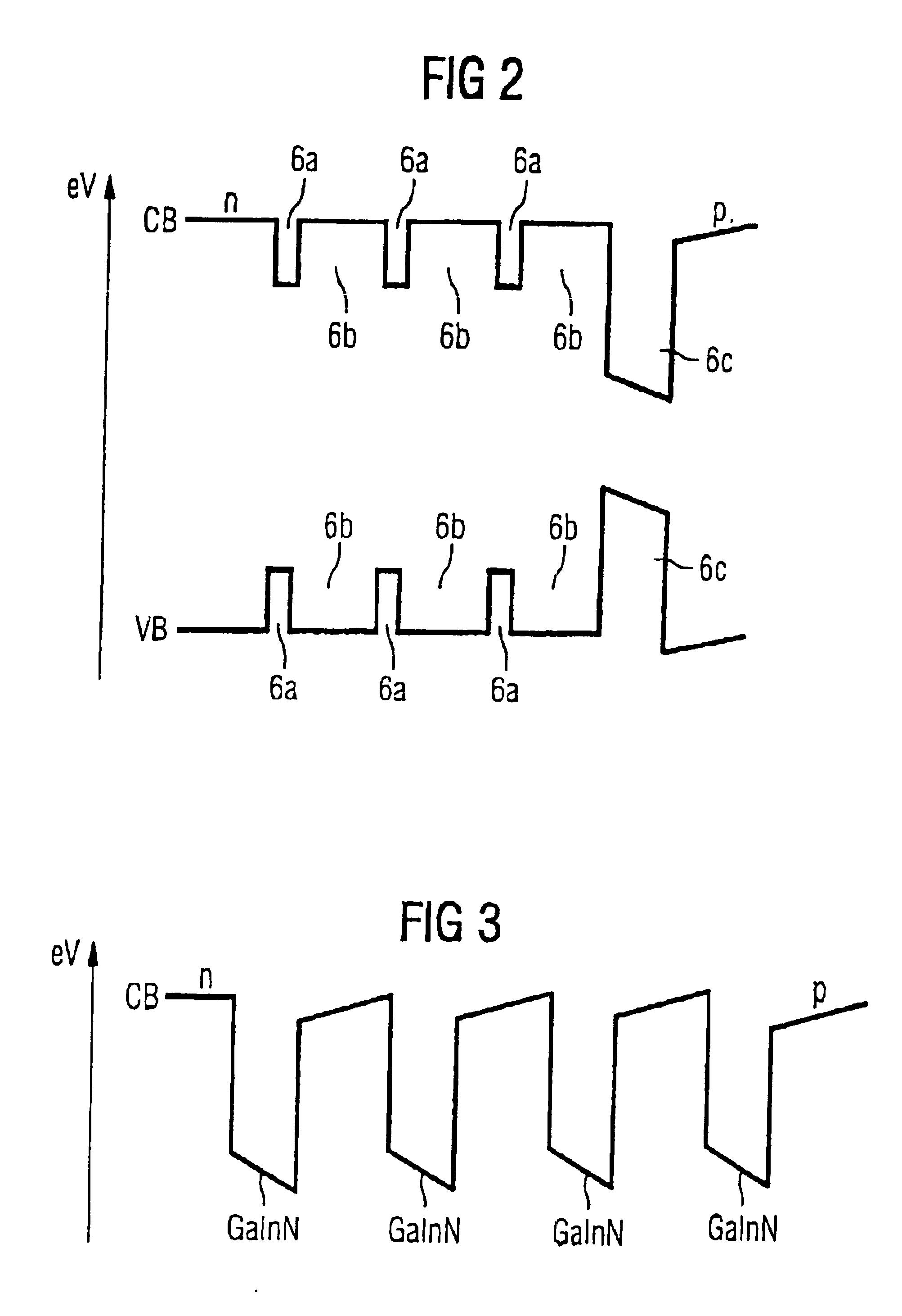
The right-hand side of the layer structure shows in a schematically indicated manner the band gap o...


PUM


Abstract

An optical semiconductor device with a multiple quantum well structure, is set out in which well layers and barrier layers, comprising various types of semiconductor layers, are alternately layered. The device well layers comprise a first composition based on a nitride semiconductor material with a first electron energy. The barrier layers comprise a second composition of a nitride semiconductor material with electron energy which is higher in comparison to the first electron energy. The well and barrier layers are in the direction of growth, by a radiation-active quatum well layer which with the essentially non-radiating well layers (6a) and the barrier layers (6b), arranged in front, form a supperlattice.

Description

BACKGROUND OF THE INVENTIONThe invention relates to an optical semiconductor device with a multiple quantum well structure, in which well layers and barrier layers comprising various types of semiconductor layers are alternately layered.A device of this type is known for example from EP 0 666 624 B1 or from the Journal of Crystal Growth 189 / 190 (1998) pages 786-789.The high quantum efficiency of indium-gallium-nitride (InGaN)-based LEDs and laser diodes is caused by the self-organized growth of indium-rich islands in the active quantum well. As a result, the injected charge carriers are spatially localized at these islands and are prevented from non-radiating recombination at lattice defects.The nucleation of these quantum dots must be initiated by suitable buffer layers. In particular, indium-containing structures are suitable before the actual active zone as a buffer layer. Indium-containing nitridic semiconductors (GaxAlyInl-(x+y)N semiconductors) have a tendency toward segregati...

Claims


Application Information

Patent Timeline
IPC IPC(8): H01S5/343H01L33/00H01S5/00H01S5/34H01L33/06H01L33/32
CPCB82Y20/00H01L33/06H01S5/34333H01L33/32H01S5/3407H01S5/3408
Inventor HARLE, VOLKERHAHN, BERTHOLDLUGAUER, HANS-JURGENBOLAY, HELMUTBADER, STEFANEISERT, DOMINIKSTRAUSS, UWEVOLKL, JOHANNESZEHNDER, ULRICHLELL, ALFREDWEIMER, ANDREAS
Owner OSRAM OLED
Why Eureka
Try Eureka