
Method of improving PMOS performance in a contact etch stop layer process

Active Publication Date: 2013-10-29
SHANGHAI HUALI MICROELECTRONICS CORP
View PDF1 Cites 3 Cited by
  • Summary
  • Abstract
  • Description
  • Claims
  • Application Information

AI Technical Summary

Benefits of technology

The present invention provides a method for improving the performance of PMOS devices in a contact etch stop layer (CESL) process. The method involves sequentially forming layers of silicon dioxide and silicon nitride on the semiconductor wafer with PMOS and NMOS devices. The silicon nitride layer contains hydrogen. The second layer of silicon dioxide is then etched to remove it over the NMOS devices while leaving it over the PMOS devices. The technical effect of this method is to improve the performance of PMOS devices without compromising the performance of NMOS devices in the CESL process.

Problems solved by technology

Specifically, a compressive liner will enhance the hole mobility of PMOS devices and thus will significantly improve performance thereof, whilst a tensile liner will reduce the hole mobility of PMOS devices and thus will degrade performance thereof.
Similarly, a tensile liner will enhance the electron mobility of NMOS devices and thus will significantly improve performance thereof, whilst a compressive liner will reduce the electron mobility of NMOS devices and thus will degrade performance thereof.
Nevertheless, this CESL process has an extremely high complexity.
As indicated above, because NMOS and PMOS devices need opposite types of stress for performance improvement, beneficial effects of such stress generation films for NMOS devices were always accompanied with disadvantageous effects on the performance of PMOS devices.

Method used


Image

  • Method of improving PMOS performance in a contact etch stop layer process
  • Method of improving PMOS performance in a contact etch stop layer process
  • Method of improving PMOS performance in a contact etch stop layer process

Examples


Embodiment Construction

[0029]Upon reading the following description of specific embodiments in conjunction with the accompanying drawing figures, the concepts of the present invention will be clearer and easier to be understood. The PMOS / NMOS device mentioned below could be a PMOS / NMOS transistor, a PMOS / NMOS Field Effect Transistor or other PMOS / NMOS structures.

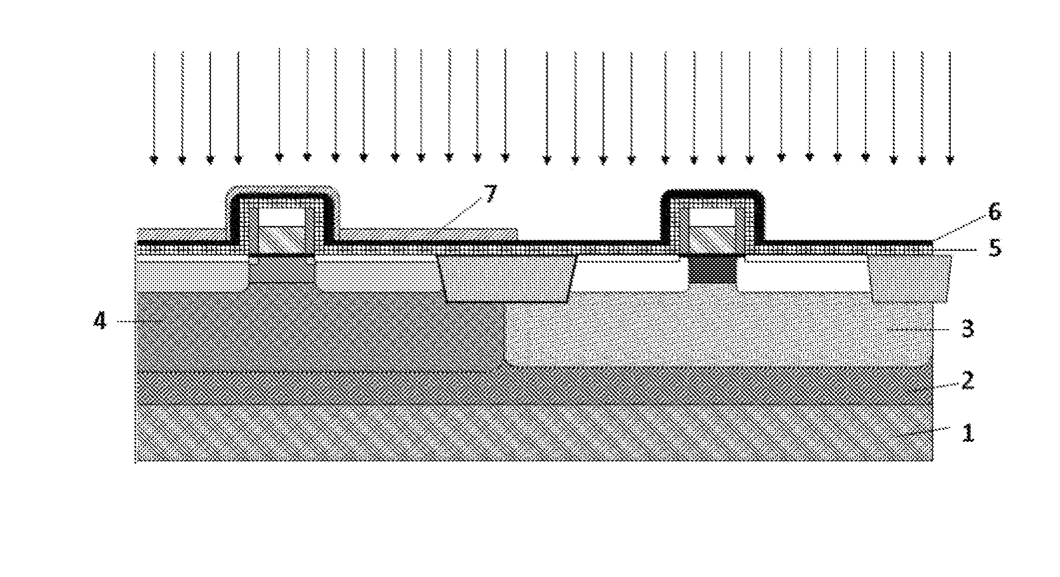
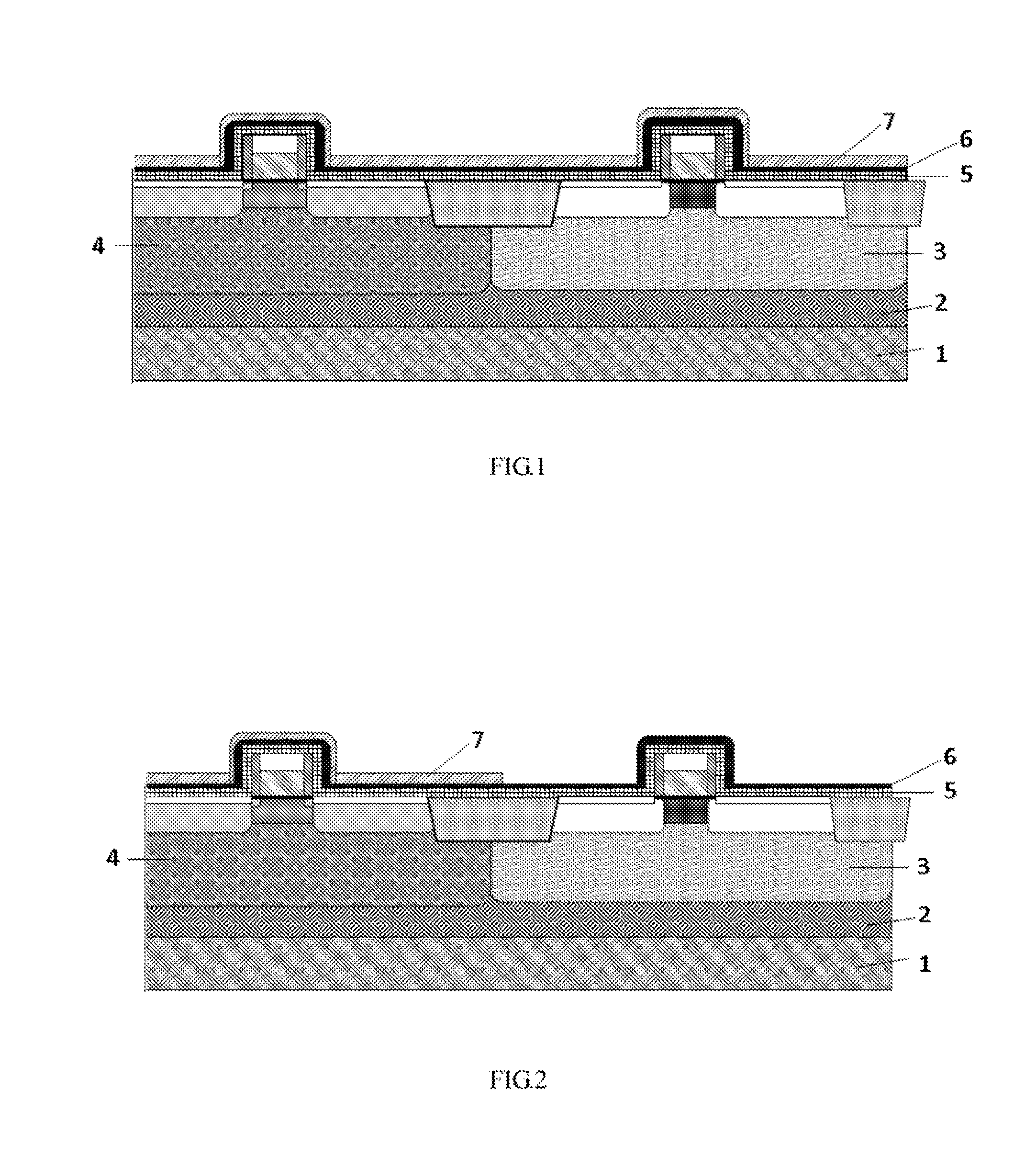
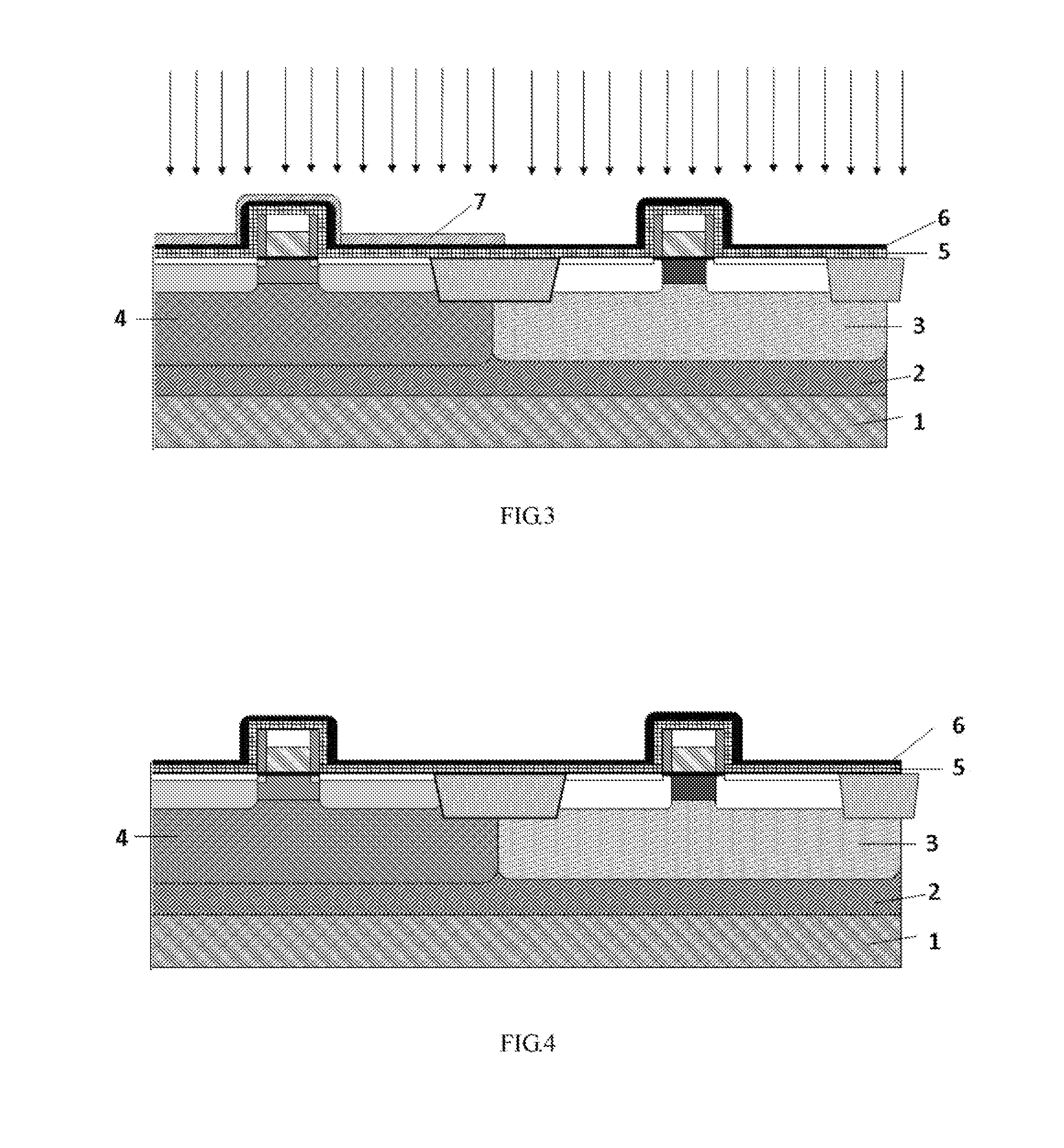
[0030]A method of improving p-type metal-oxide-semiconductor (PMOS) performance in a contact etch stop layer (CESL) process according to an embodiment of the present invention will be described below with reference to FIGS. 1 to 4.

[0031]As shown in FIGS. 1 to 4, the method according to the embodiment of the present invention includes the steps as follows.

[0032]At first, a first step is performed to sequentially form a first silicon dioxide layer 5, a hydrogen-containing silicon nitride layer 6 and a second silicon dioxide layer 7 on a semiconductor wafer having at least one PMOS device and at least one NMOS device formed thereon.

[0033]Specifically...


PUM


Abstract

A method of improving PMOS performance in a contact etch stop layer process is disclosed. The method includes: a first step for sequentially forming a first silicon dioxide layer, a hydrogen-containing silicon nitride layer and a second silicon dioxide layer on a semiconductor wafer; a second step for etching the second silicon dioxide layer; a third step for irradiating the resulting structure obtained after the step 2 with ultra-violet light; and a fourth step for removing the portions of the second silicon dioxide layer remained over the PMOS devices. By irradiating the low-stress silicon nitride layer deposited over the NMOS devices by UV light, a high tensile stress is generated in the silicon nitride over the NMOS devices while there is no high tensile stress in the silicon nitride over the PMOS devices, thus reducing disadvantageous effects of the CESL process on the performance of PMOS devices.

Description

CROSS-REFERENCES TO RELATED APPLICATIONS[0001]This application claims the priority of Chinese patent application number 201210169475.4, filed on May 28, 2012, the entire contents of which are incorporated herein by reference.TECHNICAL FIELD[0002]The present invention relates to semiconductor fabrication, and more particularly, to a method of improving PMOS performance in a contact etch stop layer (CESL) process.BACKGROUND[0003]With the development of CMOS (complementary metal oxide semiconductor) process and the continuous downscaling of CMOS devices, stress engineering has been playing a more and more importance role in semiconductor processes and device performance. Introduction of stress into CMOS devices is mainly for carrier mobility enhancement, but different types of stresses will have different effects on carrier mobility of the device.[0004]Specifically, a compressive liner will enhance the hole mobility of PMOS devices and thus will significantly improve performance thereo...

Claims


Application Information

Patent Timeline
IPC IPC(8): H01L21/8234
CPCH01L21/3105H01L21/823807H01L21/823864H01L29/7833H01L29/7843
Inventor ZHOU, JUN
Owner SHANGHAI HUALI MICROELECTRONICS CORP
Learn More