Method of fabricating porous film structure using dry processes and porous film structures fabricated by the same

a technology of porous film and dry process, which is applied in the direction of transportation and packaging, chemistry apparatus and processes, paper/cardboard articles, etc., can solve the problems of high environmental impact, difficult to actually commercialize and mass produce mesoporous thin film structures, and high process control effort. , to achieve the effect of facilitating process control

Inactive Publication Date: 2013-02-28
KOREA INST OF SCI & TECH
View PDF2 Cites 43 Cited by
  • Summary
  • Abstract
  • Description
  • Claims
  • Application Information

AI Technical Summary

Benefits of technology

The present invention provides a way to make a thin layer with small holes that can be controlled more easily without going through a wet process. This makes it better than existing methods where samples have to go through water during this step.

Problems solved by technology

The technical problem addressed in this patent is how to efficiently and commercially fabricate a mesoporous thin film structure without the drawbacks of current methods like electrochemical electrodeposition and dealloying. Additionally, there are challenges related to forming patterns on a substrate through a dry etching process involving removal of certain elements from the substrate.

Method used


Image

  • Method of fabricating porous film structure using dry processes and porous film structures fabricated by the same
  • Method of fabricating porous film structure using dry processes and porous film structures fabricated by the same
  • Method of fabricating porous film structure using dry processes and porous film structures fabricated by the same

Examples


example 1

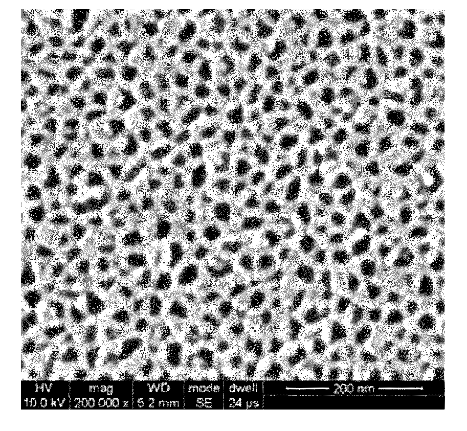
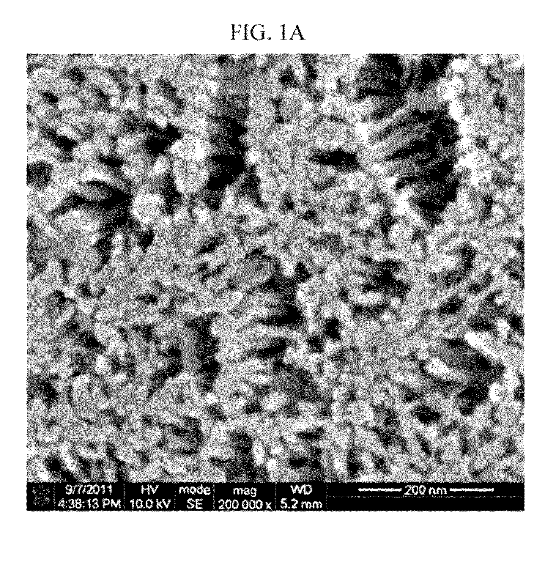
[0039]To form a thin film structure including at least two elements, Pt and Si were sputter-deposited at the same time. First, a Ti adhesive layer was deposited on a surface of an n-doped Si (100) wafer to 3 nm, and a Pt underlayer was then deposited to 30 nm. Next, a Pt—Si cosputter thin film was deposited to 150 nm. Positions of a Pt target and an Si target and their distances from a sample were adjusted so that a content of Si in the Pt—Si thin film could reach 80% by volume.

[0040]To remove elemental Si from the thin film, the thin film was etched for 30 seconds at a XeF2 pressure of 1 Ton using a non-plasma-type XeF2 dry etcher, thereby removing Si in the thin film. FIG. 1A and FIG. 1B are scanning electron microscope images of a Pt porous thin film obtained by this method. FIG. 1A shows the fabricated porous thin film from the top (top view), and FIG. 1B shows the fabricated porous thin film in cross-section from the side (cross-sectional view). With the reference to FIG. 1A, i...

example 2

[0042]A Pt—Si cosputter thin film having a thickness of 100 nm was fabricated in the same manner as in Example 1. Thereafter, the Pt—Si cosputter thin film was dry-etched using a plasma-type RIE method. SF6 gas was converted into plasma at 50 mTorr and an RF power of 200 W, and Si was then removed by dry-etching for 1 minute. Also, O2 gas was converted into plasma under the same conditions, and the plasma cleaning was performed together. FIG. 2 is a top view of the Pt porous thin film obtained via this method. It can be seen that the thin film had a porous structure having a size of approximately 10 nm.

example 3

[0043]An Au—Si cosputter thin film having a thickness of 200 nm was fabricated in the same manner as in Example 1. Thereafter, the Au—Si cosputter thin film was dry-etched for 1 minute in the same manner as in Example 1 using non-plasma-type XeF2 dry etcher to remove elemental Si. FIG. 3 is a top view of the Au porous thin film obtained via this method. It can be seen that the thin film showed similar porosity as in Example 1, but had a porous structure having a size of 10 nm to several tens of nanometers.


PUM

PropertyMeasurementUnit
Thicknessaaaaaaaaaa
Sizeaaaaaaaaaa
Structureaaaaaaaaaa

Abstract

Provided are a method of fabricating a porous thin film structure, by forming a thin film from at least two elements, followed by selectively removing the certain element using a dry etching process, and a porous thin film structure fabricated by the same. Because all processes of the method of fabricating a porous thin film structure are dry processes, process control is simply accomplished, environmental impact is low, and mass production is possible, in contrast to when using a typical wet process such as electrodeposition or dealloying. Also, since a level of porosity is easily controlled and maintained uniform, a mesoporous thin film structure showing a reproducible level of sensitivity when used as a sensor can be fabricated.

Description


Claims


Application Information

Patent Timeline
Owner KOREA INST OF SCI & TECH
Why Eureka
Try Eureka