Method for manufacturing light-emitting device

Inactive Publication Date: 2013-02-28
SUMITOMO CHEM CO LTD
View PDF2 Cites 2 Cited by
  • Summary
  • Abstract
  • Description
  • Claims
  • Application Information

AI Technical Summary

Benefits of technology

The present invention provides a method for easily making a light-emitting device by removing a thin film outside the light-emitting region using ink application. This method simplifies the manufacturing process and improves the efficiency of the device.

Problems solved by technology

This is because the ink applied for film forming to the region outside the light-emitting region potentially leads to degradation in the features of the display device.
In the case where the ink covers a trace that is provided outside the light-emitting region on the supporting substrate, the trace might be undesirably short-circuited.

Method used


Image

  • Method for manufacturing light-emitting device
  • Method for manufacturing light-emitting device
  • Method for manufacturing light-emitting device

Examples


Embodiment Construction

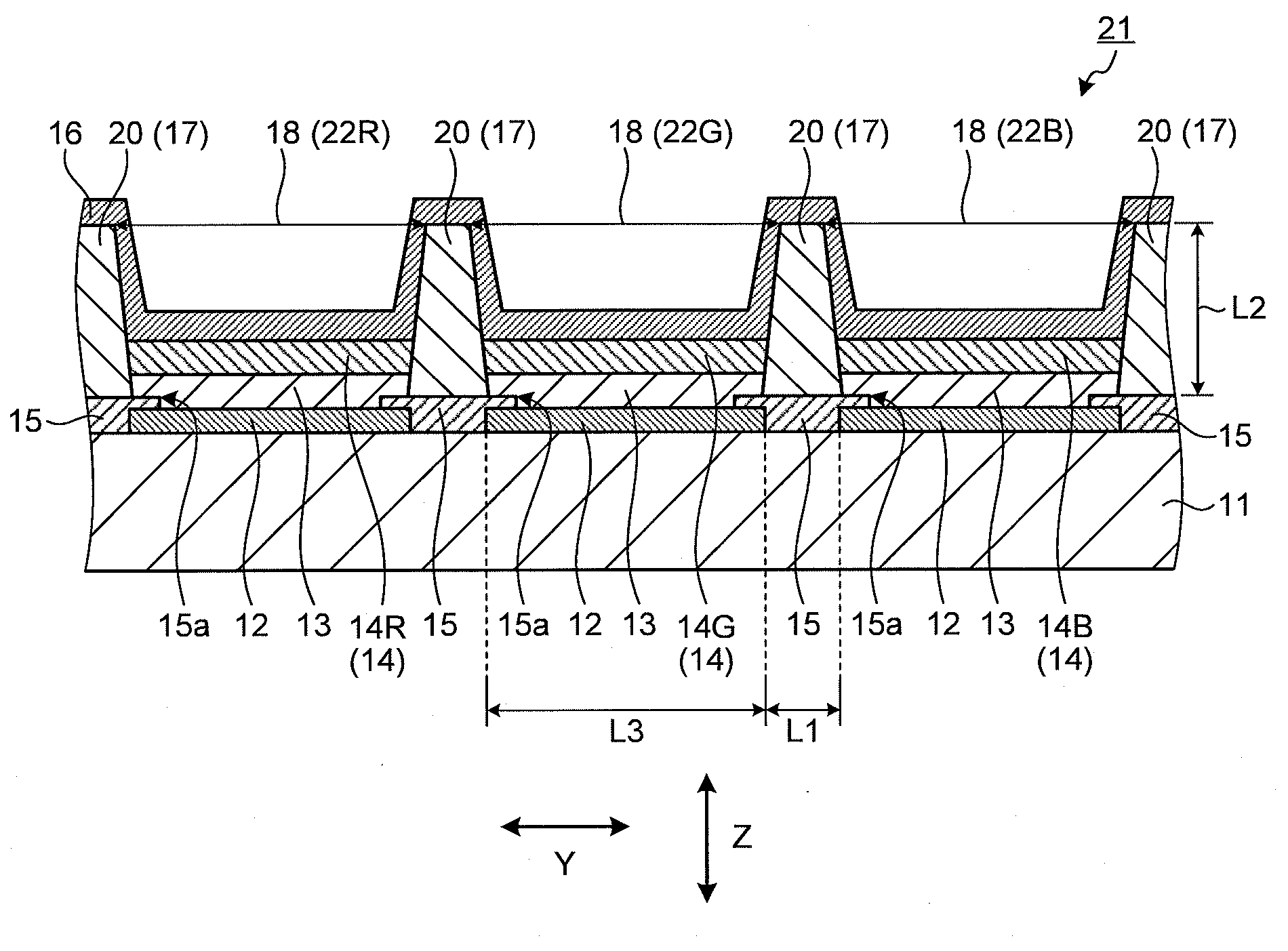
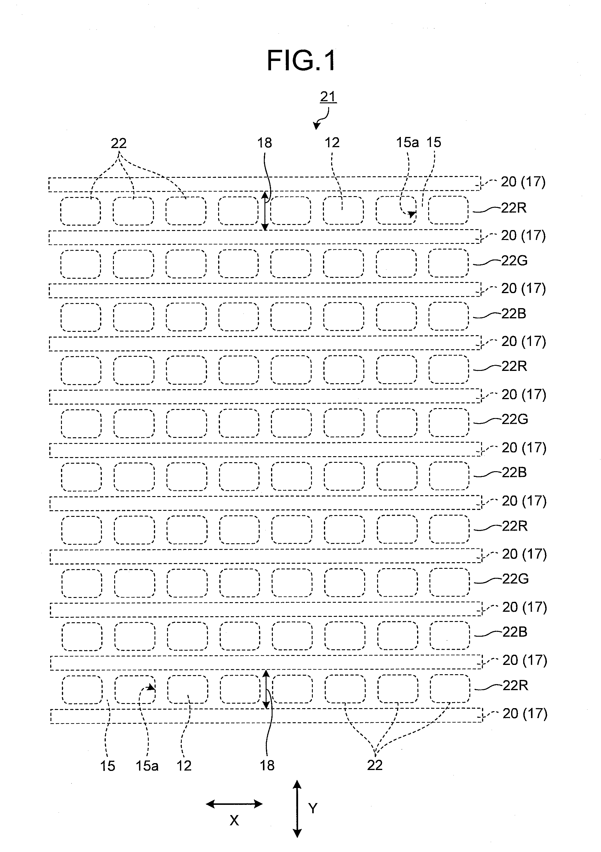
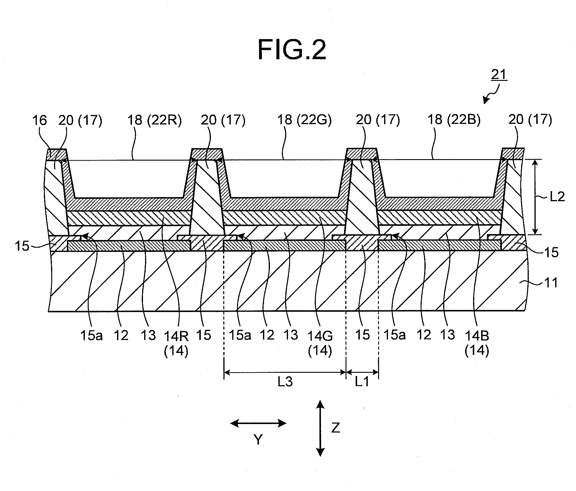
[0038]An embodiment of the present invention will be described below referring to drawings. In the description below, the shapes, the sizes, and the arrangements of constituents in each drawing are schematically illustrated to the extent to enable understanding of the invention, and the present invention is not particularly limited by these. The same constituent in each drawing is sometimes illustrated with the same reference numeral to omit an overlapping explanation.

[0039]A method for manufacturing a display device of the present invention is a method for manufacturing a light-emitting device that comprises a supporting substrate and a plurality of organic EL elements that are provided at a light-emitting region defined on the supporting substrate, the element comprising a first electrode, a second electrode, and an organic EL layer provided between the first electrode and the second electrode. The method comprises: preparing the supporting substrate that is provided with the firs...


PUM


Abstract

Manufacture of a light-emitting device by selectively removing a thin film that is formed outside a light-emitting region by ink application. The light-emitting device includes a supporting substrate and a plurality of organic electroluminescent (EL) elements (22) that are provided at a light-emitting region defined on the supporting substrate, the element including a first electrode (12), a second electrode, and an organic EL layer provided between the first electrode and the second electrode. The method includes: preparing the supporting substrate that is provided with the first electrode, supplying an ink containing the material of the organic EL layer onto the supporting substrate to form a thin film made of the ink in the light-emitting region and a region outside the light-emitting region on the supporting substrate, making the thin film in the light-emitting region insoluble, removing the thin film outside the light-emitting region by cleaning, and forming the second electrode.

Description

TECHNICAL FIELD[0001]The present invention relates to a method for manufacturing a light-emitting device.BACKGROUND ART[0002]There are various display devices with different structures and principles, and one of these display devices in which an organic electroluminescent (organic EL) element works as a light source for a pixel is currently directed toward practical use.[0003]This display device comprises a plurality of organic EL elements arranged on a supporting substrate. On the supporting substrate, a partition is generally provided for defining a compartment in which the organic EL element is provided. The organic EL elements are provided in proper alignment each in the compartment defined by the partition.[0004]FIG. 4 schematically illustrates an aspect to supply an ink by a nozzle printing method. As illustrated in FIG. 4, for example, where a partition 2 composed of a plurality of partition members 1 extending in a prescribed line direction X is provided on a supporting subs...

Claims


Application Information

Patent Timeline
IPC IPC(8): H01L51/56
CPCH01L27/3246H01L27/3283H01L51/0004H01L51/0015H01L51/0005H10K59/173H10K71/13H10K71/135H10K59/122H10K71/211H05B33/10H10K71/00
Inventor GODA, TADASHI
Owner SUMITOMO CHEM CO LTD
Why Eureka
Try Eureka