Encapsulating sheet, producing method thereof, light emitting diode device, and producing method thereof

a technology of light-emitting diodes and encapsulating sheets, which is applied in the direction of manufacturing tools, point-like light sources, lighting and heating apparatus, etc., can solve the problems of low production efficiency and large number of production steps, and achieve the effect of suppressing the occurrence of color unevenness of light in the light-emitting diodes and brightness differences

Active Publication Date: 2013-03-14
EPISTAR CORP
View PDF1 Cites 28 Cited by
  • Summary
  • Abstract
  • Description
  • Claims
  • Application Information

AI Technical Summary

Benefits of technology

[0028]As a result, in the light emitting diode device, the light emitting diode element can be surely allowed to serve as a surface light source. That is, a difference in brightness between an immediate upper portion o...

Problems solved by technology

On the other hand, in the method for producing a light emitting diode device in Japanese Unexamined Patent Publication No. 2007-67204, there is a disadvantage that the light emitting diode chip is encapsulated by the tr...

Method used


Image

  • Encapsulating sheet, producing method thereof, light emitting diode device, and producing method thereof
  • Encapsulating sheet, producing method thereof, light emitting diode device, and producing method thereof
  • Encapsulating sheet, producing method thereof, light emitting diode device, and producing method thereof

Examples


example 1

[0269](1) Formation of Light Scattering Layer

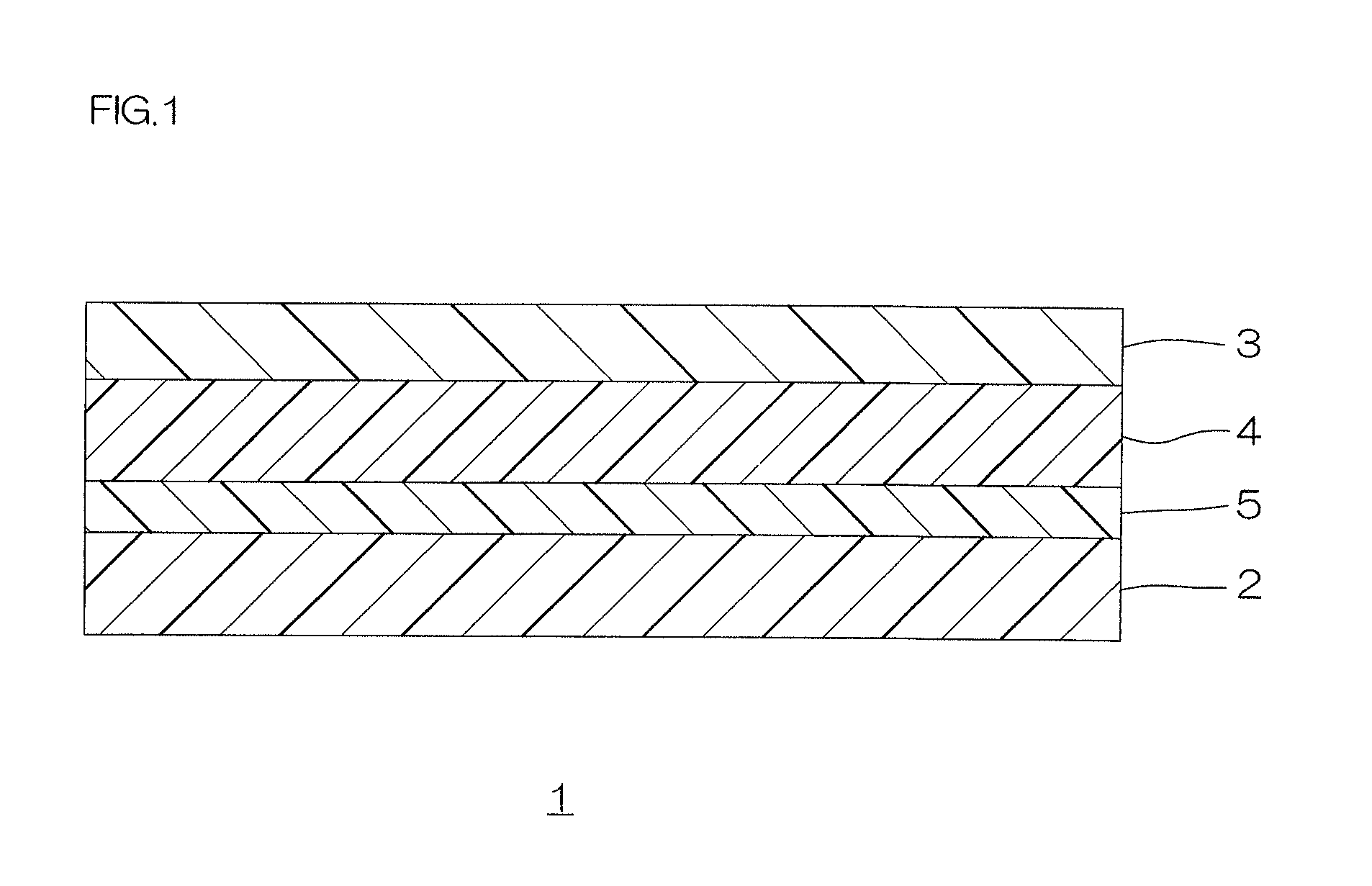
[0270]5 g of silicon dioxide (FB-3SDC, in a sphere shape, an average particle size of 3.4 μm, manufactured by DENKI KAGAKU KOGYO KABUSHIKI KAISHA.) was added to 5 g of a silicone elastomer (ELASTOSIL LR-7665, manufactured by WACKER ASAHIKASEI SILICONE CO., LTD.) to be uniformly dispersed by hand stirring, so that a light scattering resin composition in a liquid state was prepared. Thereafter, the prepared light scattering resin composition was subjected to a defoaming process and subsequently, the defoamed product was applied on a separator film (SS4C) so as to have a thickness of 500 μm using an applicator. Thereafter, the obtained film was cured by heating at 100° C. for 10 minutes, so that a light scattering layer made from a light scattering resin in a C-stage (completely cured) state was formed (ref: FIG. 2(a)).

[0271](2) Formation of Spacer Layer

[0272]A thermosetting silicone resin composition made from the defoamed silicone elastome...

example 2

[0296]A phosphor layer and an encapsulating layer were sequentially formed to form an encapsulating sheet and subsequently, a light emitting diode device was produced in the same manner as in Example 1, except that the thickness of a spacer layer was changed from 1 mm to 2 mm in (2) Formation of Spacer Layer.

example 3

[0297]A phosphor layer and an encapsulating layer were sequentially formed to form an encapsulating sheet and subsequently, a light emitting diode device was produced in the same manner as in Example 1, except that the thickness of a spacer layer was changed from 1 mm to 3 mm in (2) Formation of Spacer Layer.


PUM

PropertyMeasurementUnit
Thicknessaaaaaaaaaa
Thicknessaaaaaaaaaa
Thicknessaaaaaaaaaa

Abstract

An encapsulating sheet includes an encapsulating layer for encapsulating a light emitting diode element, a light scattering layer formed at one side in a thickness direction of the encapsulating layer and for scattering light emitted from the light emitting diode element, and a spacer layer interposed between the encapsulating layer and the light scattering layer.

Description

CROSS-REFERENCE TO RELATED APPLICATION[0001]The present application claims priority from Japanese Patent Application No. 2011-200579 filed on Sep. 14, 2011, the contents of which are hereby incorporated by reference into this application.BACKGROUND OF THE INVENTION[0002]1. Field of the Invention[0003]The present invention relates to an encapsulating sheet, a producing method thereof, a light emitting diode device, and a producing method thereof, to be specific, to a light emitting diode device used for optical use, a producing method thereof, an encapsulating sheet used therein, and a producing method thereof.[0004]2. Description of Related Art[0005]In a light emitting diode device capable of emitting high-energy light, for example, an LED (a light emitting diode element) and an encapsulating layer which encapsulates the LED are provided. In the light emitting diode device, light emitted from the LED transmits through the encapsulating layer.[0006]The LED emits light with high direc...

Claims


Application Information

Patent Timeline
IPC IPC(8): F21V7/00B23P11/00F21V13/08
CPCH01L25/0753H01L33/507H01L33/52H01L33/56Y10T29/49002H01L2933/0091H01L2924/0002H01L2933/005H01L2924/00H01L33/48
Inventor KONDO, TAKASHIMATSUDA, HIROKAZUKONO, HIROKI
Owner EPISTAR CORP
Why Eureka
Try Eureka