Method of burn-in test of eeprom or flash memories

a technology of flash memory and burn-in test, which is applied in the direction of read-only memories, instruments, and static storage, etc., can solve the problems of increasing the failure rate, the voltage swg may not be higher, and the gate oxide breakdown of transistors, etc., to avoid programming non-addressed memory cells. , to achieve the effect of increasing the tim

Active Publication Date: 2013-03-14
STMICROELECTRONICS (ROUSSET) SAS
View PDF6 Cites 2 Cited by
  • Summary
  • Abstract
  • Description
  • Claims
  • Application Information

AI Technical Summary

Benefits of technology

[0016]To compensate for the small difference between test voltages and normal operation voltages, it is known to increase the time during which each transistor to be tested is subjected to a test voltage. This solution also has a limit since it cannot be considered to penalize production rates by increasing burn-in test durations beyond an acceptable limit.

Problems solved by technology

One of the main causes of failure of an EEPROM memory is gate oxide breakdown of transistors which may be subjected to a relatively high voltage.
The rate of failure tends to increase with memory miniaturization.
In practice, voltage SWG may not be higher to avoid programming non-addressed memory cells.
However, the test voltages should not be chosen too close to this intrinsic breakdown voltage to avoid discarding circuits having acceptable defects.
At voltages superior or equal to this value, leaks may also appear between the drain and source of these transistors.
It is therefore not possible to subject these transistors to voltages significantly higher than normal operating voltages (VPP−SWG=12 V).
However, the weakness of N-channel MOS transistors is between the drain and source, whose voltage cannot exceed 17 V in the blocked state.
Although the gate oxides of transistors considered to be of sufficient quality may support 17 V, it is not possible to go beyond 14 V due to the presence of P-channel transistors in the blocked state whatever the state of the circuit.
This solution also has a limit since it cannot be considered to penalize production rates by increasing burn-in test durations beyond an acceptable limit.

Method used


Image

  • Method of burn-in test of eeprom or flash memories
  • Method of burn-in test of eeprom or flash memories
  • Method of burn-in test of eeprom or flash memories

Examples


Embodiment Construction

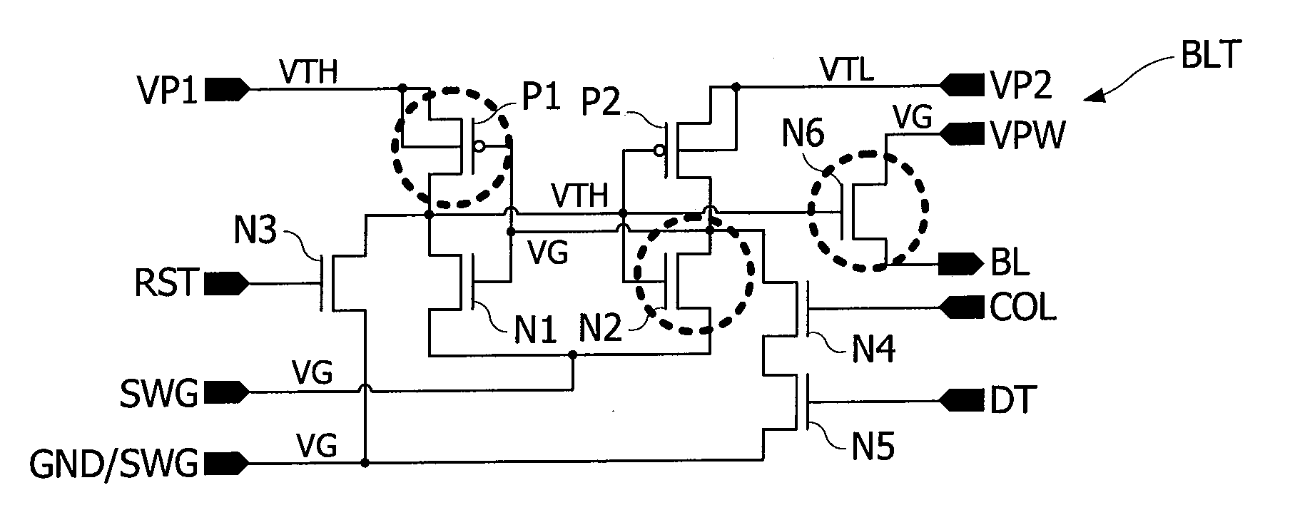
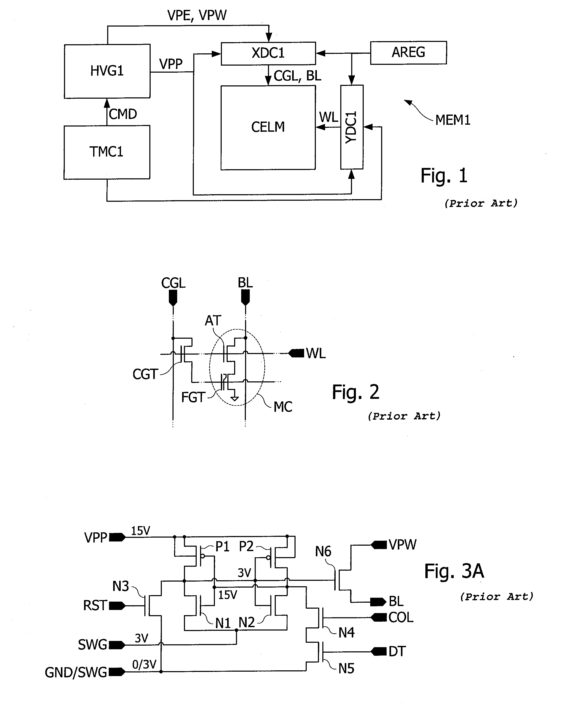
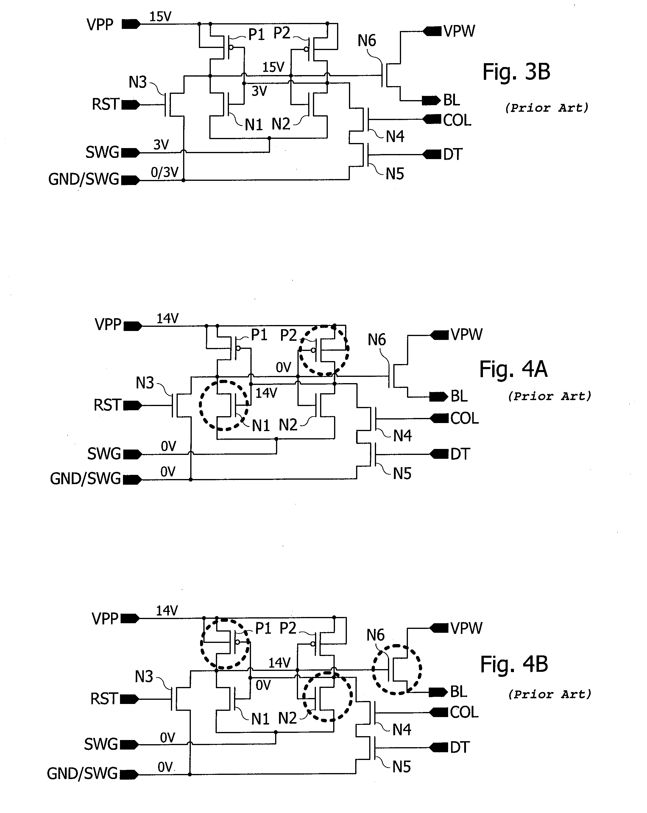
[0043]FIG. 5 shows an EEPROM memory referred to as MEM, according to one embodiment. Memory MEM comprises a memory array CELM comprising memory cells distributed into lines and columns transverse to lines. Line YDEC and column XDEC decoders allow one or more words comprising several memory cells of a same line to be selected. Decoders XDEC, YDEC are controlled by an address register AREG allowing a word at the intersection of a line and a group of columns to be selected. A high voltage generation circuit VPGN supplies a high voltage VPP and voltages VPE, VPW to decoder XDEC. Decoders XDEC, YDEC control memory cells for reading, programming or erasing by providing adapted voltages, to bit lines BL, and gate control lines CGL for decoder XDEC, and word lines WL for decoder YDEC. A mode control circuit TMCL transmits a control signal CMD to the circuit HVGN to activate a burn-in test mode or a normal operating mode of the memory.

[0044]According to one embodiment, the memory MEM is modi...


PUM


Abstract

The disclosure relates to a method for testing an integrated circuit, comprising in a burn-in test mode, two steps during which gate oxides of conductive high voltage MOS transistors of the integrated circuit are subjected to a first test voltage, and blocked high voltage MOS transistors of the integrated circuit are subjected to a second test voltage, the first test voltage being set to a value higher than a high supply voltage supplied to the high voltage MOS transistors in a normal operating mode, to make the gate oxides of transistors considered as insufficiently robust break down, the second test voltage being set to a value lower than the first test voltage and which can be supported by the blocked transistors, the states of the transistors being changed between the two steps.

Description

BACKGROUND[0001]1. Technical Field[0002]The present disclosure relates to burn-in tests of integrated circuits like EEPROM memories, at the end of manufacture. These tests include in particular subjecting, during some time, an integrated circuit to unfavorable operating constraints, to cause a failure of the circuit if it has some manufacture defects. That way, the integrated circuits passing such tests have a failure rate which may reach low values.[0003]2. Description of the Related Art[0004]One of the main causes of failure of an EEPROM memory is gate oxide breakdown of transistors which may be subjected to a relatively high voltage. The rate of failure tends to increase with memory miniaturization. In an EEPROM memory, such high voltage transistors are present in bit line latches, gate control latches and word line selection latches, as well as in each memory cell and in gate control switches of a group of memory cells. FIG. 1 schematically shows a conventional EEPROM memory. In...

Claims


Application Information

Patent Timeline
Patent Type & Authority Applications(United States)
IPC IPC(8): G11C16/04
CPCG11C29/06G11C29/02
Inventor TAILLIET, FRANCOIS
Owner STMICROELECTRONICS (ROUSSET) SAS
Why Eureka
Try Eureka