Supercharge Your Innovation With Domain-Expert AI Agents!

Bonding pad structure and fabricating method thereof

a technology of bonding pad and fabrication method, which is applied in the direction of semiconductor/solid-state device manufacturing, electrical apparatus, semiconductor/conductor devices, etc., can solve the problems of short-circuited problem and increase the fabricating cos

Inactive Publication Date: 2013-03-21
UNITED MICROELECTRONICS CORP
View PDF4 Cites 0 Cited by
  • Summary
  • Abstract
  • Description
  • Claims
  • Application Information

AI Technical Summary

Benefits of technology

The present invention provides a bonding pad structure for use in an integrated circuit device. The structure includes a dielectric layer, a conductor structure, a pad opening, and an isolation trench. The etch stop structure is optionally included. The conductor structure and etch stop structure can be in contact or separated from each other. The bonding pad structure can be used in the production of an integrated circuit, which includes a semiconductor substrate with a first surface and a second surface, a dielectric layer, a conductor structure, a pad opening, and an isolation trench. The method includes steps of forming a photodiode, a color filter layer, a microlens layer, a protecting layer, and a multi-layered wiring structure. The bonding pad structure and multi-layered wiring structure can be bonded to a handle wafer.

Problems solved by technology

Under this circumstance, a short-circuited problem occurs.
The additional processing step of forming the insulating layer may increase the fabricating cost.

Method used


Image

  • Bonding pad structure and fabricating method thereof
  • Bonding pad structure and fabricating method thereof
  • Bonding pad structure and fabricating method thereof

Examples


Embodiment Construction

[0029]The present invention will now be described more specifically with reference to the following embodiments. It is to be noted that the following descriptions of preferred embodiments of this invention are presented herein for purpose of illustration and description only. It is not intended to be exhaustive or to be limited to the precise form disclosed.

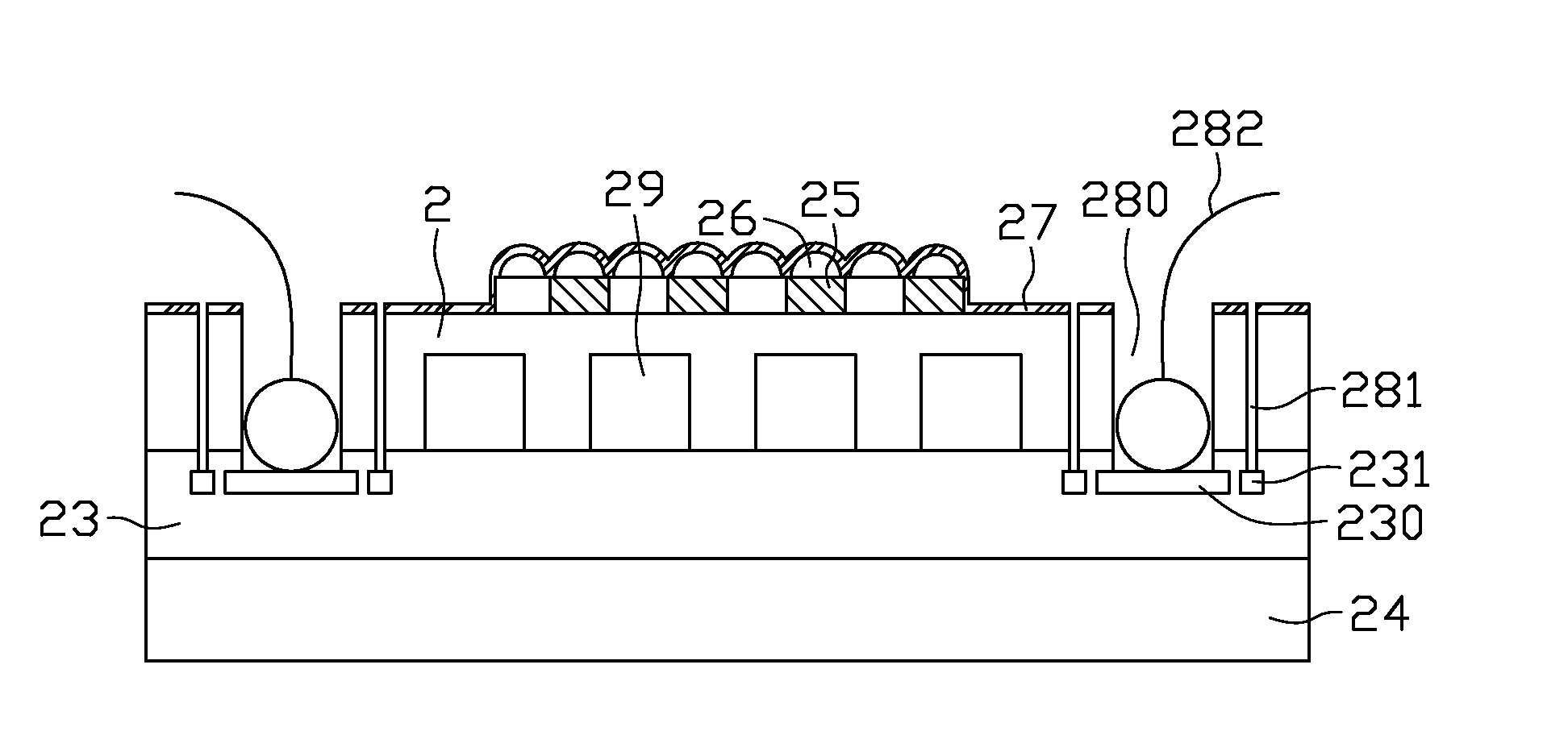
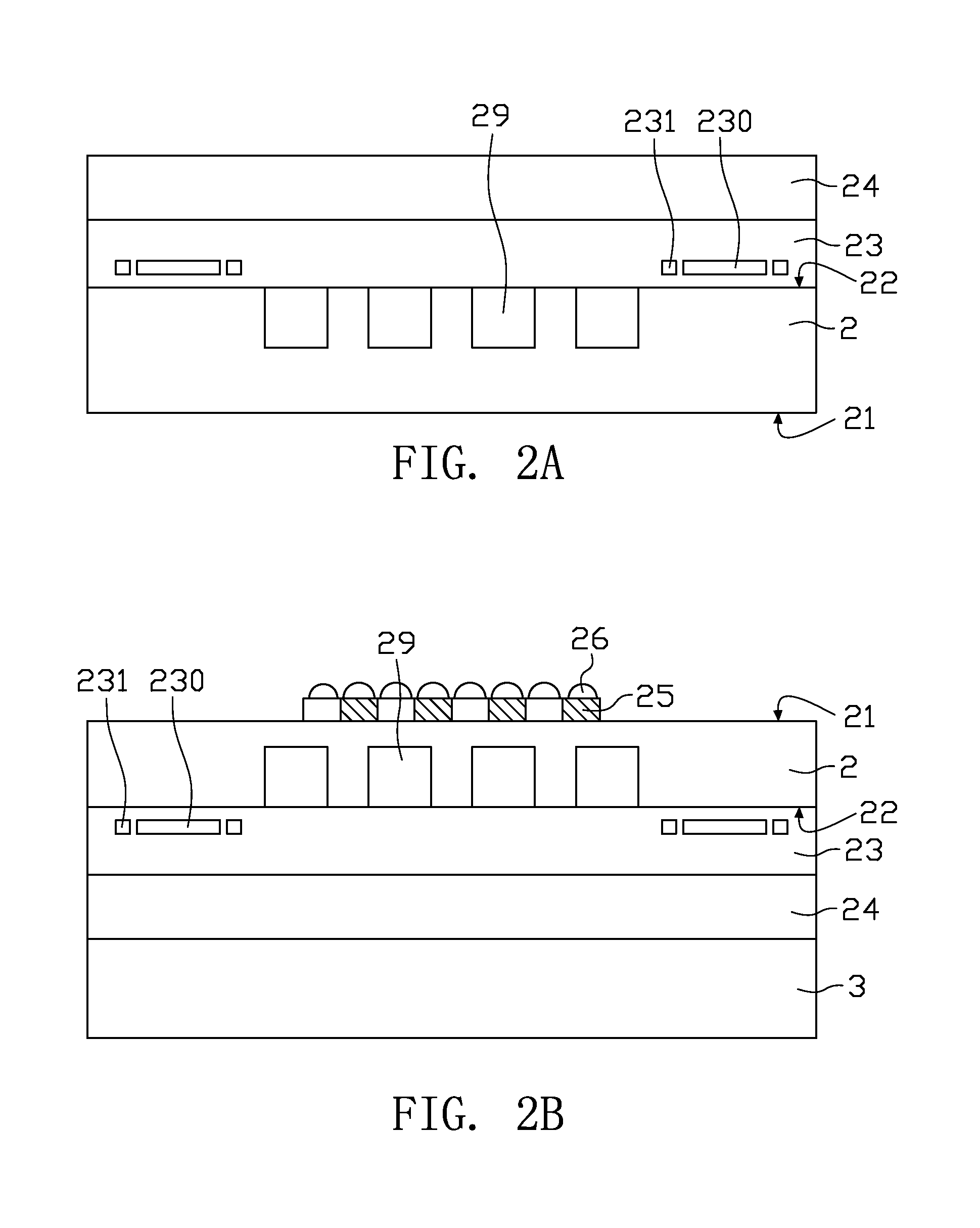
[0030]FIGS. 2A˜2E are schematic cross-sectional views illustrating a method for fabricating a bonding pad structure according to an embodiment of the present invention. The method can be applied to the production of various integrated circuit chips, especially a complementary metal oxide semiconductor image sensor.

[0031]First of all, as shown in FIG. 2A, a semiconductor substrate 2 is provided. The semiconductor substrate 2 has a first surface 21 and a second surface 22. A multi-layered wiring structure 24 including a metal wiring layer and a dielectric layer is located at the side of the second surface 22 of the semiconductor su...


PUM


Abstract

A bonding pad structure is used in an integrated circuit device. The integrated circuit device includes a semiconductor substrate with a first surface and a second surface. The bonding pad structure includes a dielectric layer, a conductor structure, a pad opening and an isolation trench. The dielectric layer is formed on the second surface of the semiconductor substrate. The conductor structure is disposed within the dielectric layer. The pad opening is formed in the first surface of the semiconductor substrate. The pad opening runs through the semiconductor substrate and a part of the dielectric layer, so that the conductor structure is exposed. The isolation trench has an opening in the first surface of the semiconductor substrate. The isolation trench runs through the semiconductor substrate and a part of the dielectric layer, and the isolation trench is disposed around the pad opening.

Description

FIELD OF THE INVENTION[0001]The present invention relates to a bonding pad structure, and more particularly to a bonding pad structure for use in an integrated circuit device. The present invention also relates to a method of fabricating such a bonding pad structure.BACKGROUND OF THE INVENTION[0002]Due to small size and low cost, a complementary metal oxide semiconductor image sensor (also referred as CIS) is widely used in various image pickup devices. FIG. 1A is a schematic cross-sectional view illustrating a conventional complementary metal oxide semiconductor image sensor fabricated by a front side illumination technology. After an incident light is transmitted through a microlens layer 11 and a color filter layer 12, the incident light is directed to a photodiode 15 in a substrate 1 through a metal wiring layer 13 and a dielectric layer 14. Since metal wiring layer 13 and the dielectric layer 14 are very thick, the light sensitivity is usually insufficient.[0003]For solving the...

Claims


Application Information

Patent Timeline
Patent Type & Authority Applications(United States)
IPC IPC(8): H01L31/0232
CPCH01L27/14603H01L27/14632H01L27/14627
Inventor KAO, CHING-HUNG
Owner UNITED MICROELECTRONICS CORP
Features
  • R&D
  • Intellectual Property
  • Life Sciences
  • Materials
  • Tech Scout
  • Unparalleled Data Quality
  • Higher Quality Content
  • 60% Fewer Hallucinations
Learn More