Touch device and manufacturing method thereof

a technology of touch device and manufacturing method, which is applied in the field of touch device, can solve the problems of misoperation of the touch device, inability of the external detection circuit to accurately detect the change in capacitance generated, etc., and achieve the effects of improving the reliability of the touch circuit, avoiding misoperation, and shielding signals

Active Publication Date: 2013-04-18
TPK TOUCH SOLUTIONS (XIAMEN) INC
View PDF4 Cites 28 Cited by
  • Summary
  • Abstract
  • Description
  • Claims
  • Application Information

AI Technical Summary

Benefits of technology

[0011]By means of the touch device and the manufacturing method provided in the present disclosure, signal interference can be shielded and misoperation can be avoided, improving the reliability for operation of the touch circuit.

Problems solved by technology

However, while using the above-mentioned different touch devices, these touch devices are easily interfered by external signals, which may lead to misoperation.
However, the change in capacitance is easily interfered by external signals or other factors, which may cause abnormal change in capacitance leading to misoperation of the touch device.
Thus, the external detection circuit is not able to accurately detect the change in capacitance generated in the sensing electrode structure 12 or the location where the change in capacitance is generated.

Method used


Image

  • Touch device and manufacturing method thereof
  • Touch device and manufacturing method thereof
  • Touch device and manufacturing method thereof

Examples


Embodiment Construction

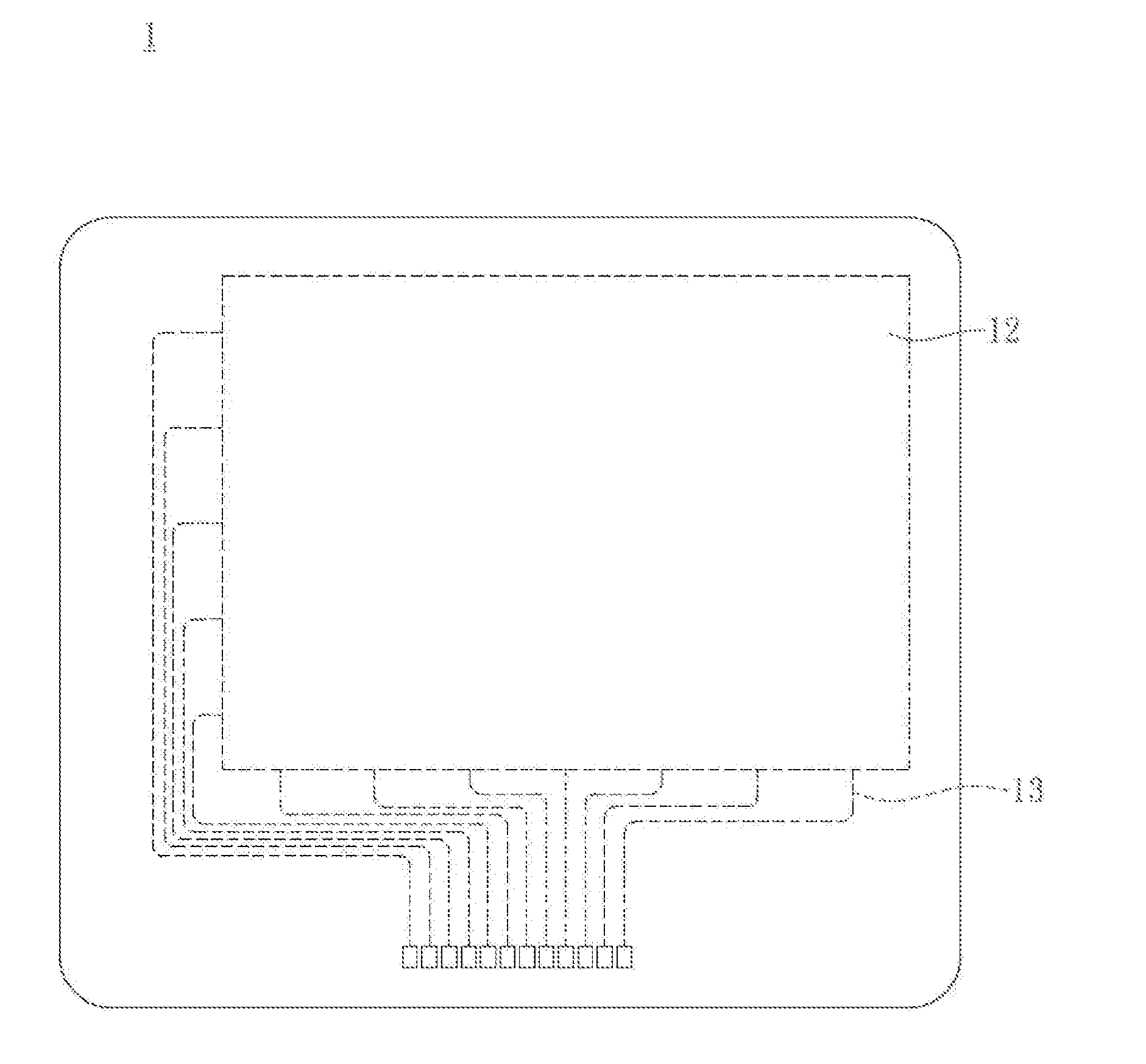
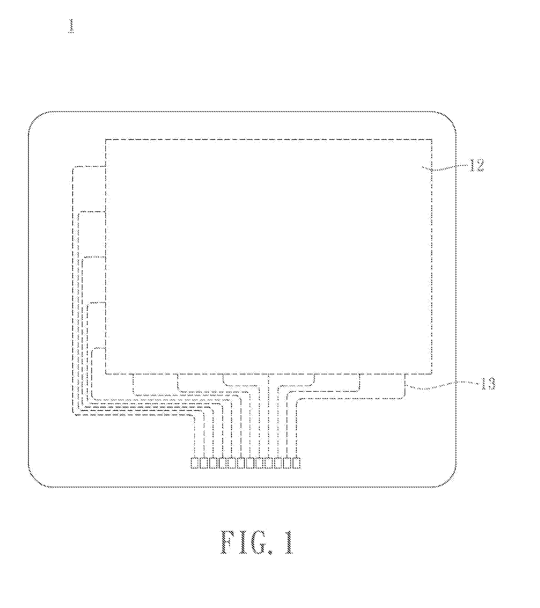
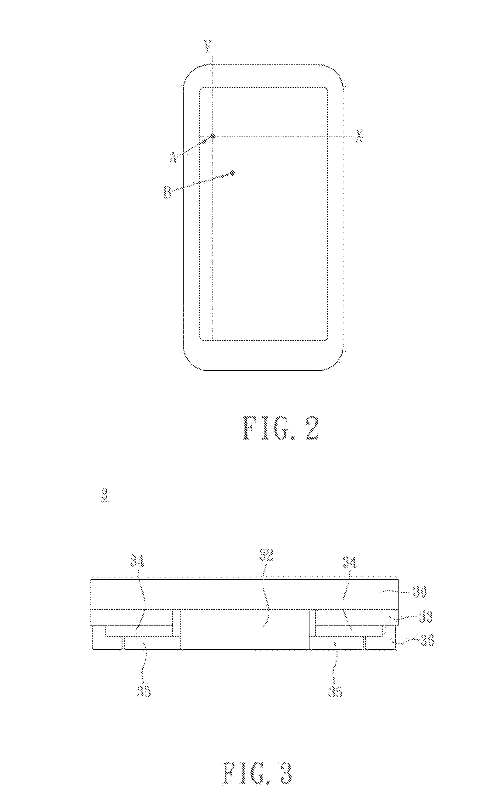
[0031]FIG. 3 is a sectional view of a touch device in accordance with an embodiment of the present disclosure. A touch device 3 mainly comprises a substrate 30, a sensing electrode structure 32, a shielding layer 33, a plurality of peripheral connection wires 35 and a grounding wire 36. The sensing electrode structure 32 is located on a lower surface of the substrate 30, wherein area covered by the sensing electrode structure 32 is defined as a touch area and area not covered by the sensing electrode structure 32 is a surrounding area. The shielding layer 33 further covers the lower surface of the substrate 30, surrounds plural sides of the sensing electrode structure 32, and is located on the surrounding area. The plurality of peripheral connection wires 35 are located under the shielding layer 33 and electrically connected to the sensing electrode structure 32. The grounding wire 36 is located under the shielding layer 33 and electrically connected to the shielding layer 33. The g...


PUM

PropertyMeasurementUnit
conductiveaaaaaaaaaa
capacitanceaaaaaaaaaa
areaaaaaaaaaaa

Abstract

The present disclosure relates to a touch technology, especially to a touch device and a manufacturing method thereof. The touch device comprises a sensing electrode structure, a shielding layer, a plurality of peripheral connection wires and a grounding wire. The shielding layer surrounds the periphery of the sensing electrode structure. The plurality of peripheral connection wires are located under the shielding layer and electrically connected to the sensing electrode structure. The grounding wire is electrically connected to the shielding layer. Thus, in accordance with the present disclosure, the touch device can shield external interference, and the reliability for operation of the touch circuit can be improved.

Description

[0001]This application claims the benefit of Chinese application No. 201110317553.X, filed on Sep. 12, 2011.BACKGROUND OF THE INVENTION[0002]1. Field of the Invention[0003]The present disclosure relates to a touch technology, especially to a touch device and a manufacturing method thereof.[0004]2. Description of the Related Art[0005]Electronic devices comprise input and output device interfaces that facilitate interaction between human beings and electronic devices. Due to rapid development of electronic components, touch input device interfaces have become popular. Conventional push-button input devices are likely to be replaced by touch input devices in near future. Touch devices used for touch inputting can be classified into various types such as resistive type, capacitive type, inductive type, acoustic wave type, optical type, etc. However, while using the above-mentioned different touch devices, these touch devices are easily interfered by external signals, which may lead to m...

Claims


Application Information

Patent Timeline
Patent Type & Authority Applications(United States)
IPC IPC(8): G06F3/041H01H11/00
CPCG06F3/044Y10T29/49105G06F2203/04103G06F3/0445G06F3/0446G06F1/1626G06F3/0412G06F2203/04107G06F2203/04113
Inventor HUANG, PINGPINGWU, JIACAI, ZHIXIONGJIANG, YAU-CHEN
Owner TPK TOUCH SOLUTIONS (XIAMEN) INC
Why Eureka
Try Eureka