

Method of embedding magnetic component in substrate
a magnetic component and substrate technology, applied in the field of embedding electronic components, can solve the problems of more difficult than other problems in holding an embedding magnetic component in a printed circuit board
- Summary
- Abstract
- Description
- Claims
- Application Information
AI Technical Summary
Benefits of technology
Problems solved by technology
Method used
Image

Examples
first embodiment
[0018]FIG. 2A, FIG. 3A, FIG. 4A and FIG. 5A are top views showing a method of embedding a magnetic component according to the present invention, wherein FIG. 2B, FIG. 3B, FIG. 4B and FIG. 5B are cross-sectional views viewed along respective dash lines I-I′ in FIG. 2A, FIG. 3A, FIG. 4A and FIG. 5A.
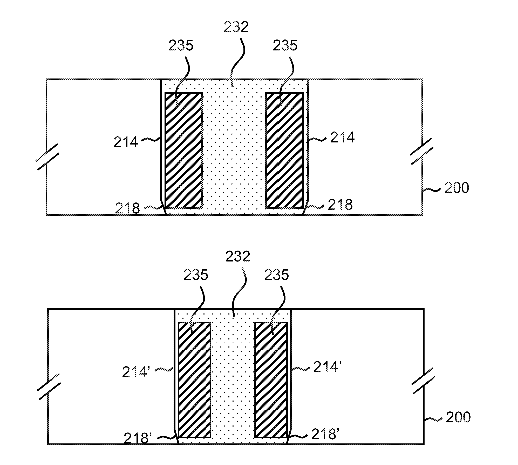
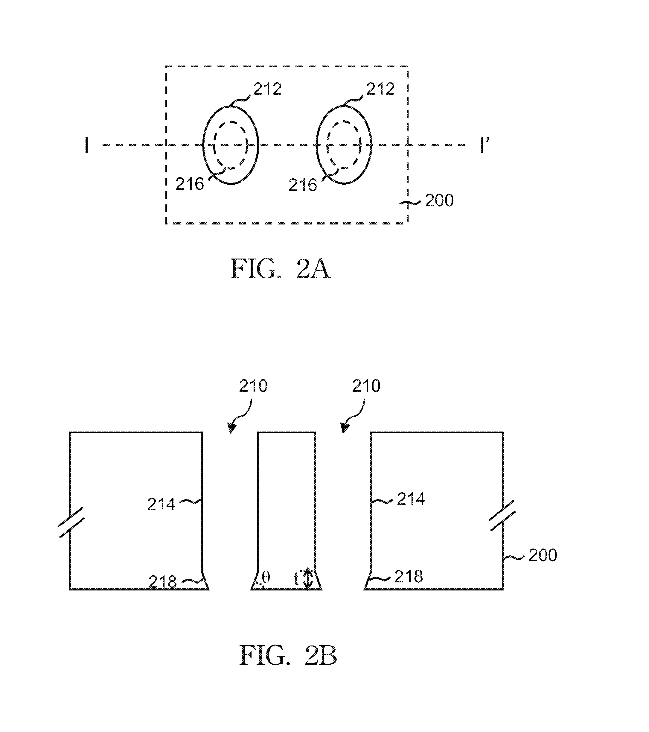
[0019]Referring to FIG. 2A and FIG. 2B, two holes 210 spaced at a certain distance are formed in a substrate 200 by mechanically drilling. The interval and depths of the two holes 210 are determined in accordance with the size and position of an embedded device. The area of a top opening 212 of each hole 210 is larger than the area of a bottom opening 216. A sidewall 214 extends from the top opening 212 vertically downwards to a predetermined depth and then is slanted inwardly to the bottom opening 216 to form a sloped sidewall 218 at the bottom of each hole 210. The substrate 200 may be an electroplated insulation substrate that covers the overlying or underlying conductive layers and is s...
second embodiment
[0026]FIG. 2A′, FIG. 3A′, FIG. 4A′ and FIG. 5A′ are top views showing a method of embedding a magnetic component according to the present invention, wherein FIG. 2B′, FIG. 3B′, FIG. 4B′ and FIG. 5B′ are cross-sectional views viewed along respective dash lines I-I′ in FIG. 2A′, FIG. 3A′, FIG. 4A′ and FIG. 5A′.
[0027]Referring to FIG. 2A′ and FIG. 2B′, two partially overlapped holes are formed in the substrate 200 by mechanically drilling to form an assembly hole 210′. The extent of overlapping and the depth of the two holes are determined in accordance with the size and position of an embedded device. The area of the top opening 212′ of the assembly hole 210′ is larger than the area of the bottom opening 216′. The sidewall 214′ extends from the top opening 212′ vertically downwards to a predetermined depth and then is slanted inwardly to the bottom opening 216′ to form a sloped sidewall 218′ at the bottom of the assembly hole 210′. The substrate 200 may be an electroplated insulation ...
third embodiment
[0033]FIG. 6AFIG. 7A, FIG. 8A and FIG. 9A are top views showing a method of embedding a magnetic component according to the present invention, wherein FIG. 6B, FIG. 7B, FIG. 8B and FIG. 9B are cross-sectional views viewed along respectively dash lines I-I′ in FIG. 6A, to FIG. 9A.
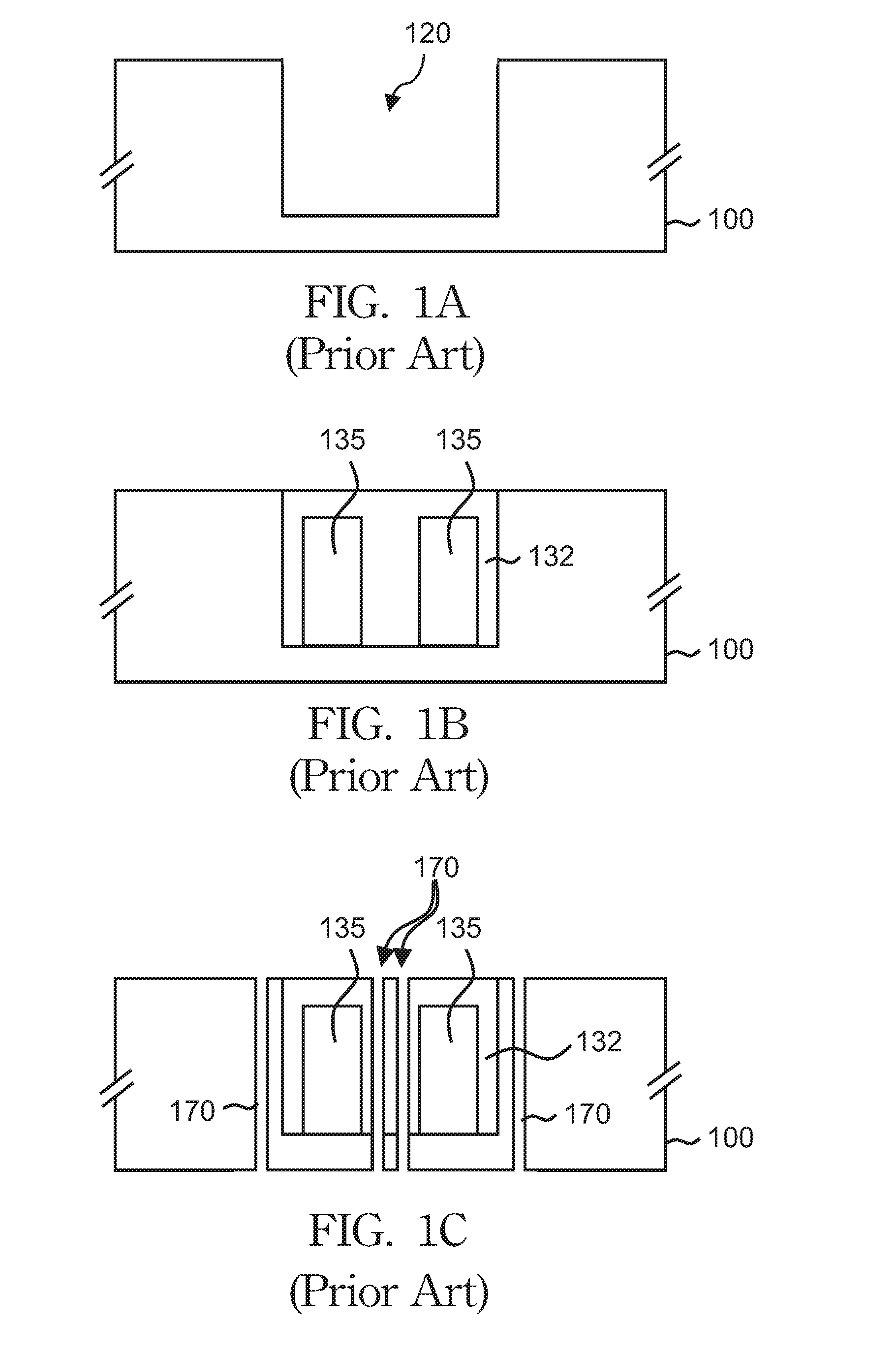
[0034]Referring to FIG. 6A and FIG. 6B, two holes 210 spaced at a certain distance are formed in the substrate 200 by mechanically drilling. The interval and depths of the two holes 210 are determined depending on the size and position of an embedded device. The area of the top opening 212 of the hole 210 is larger than the area of the bottom 217. The sidewall 214 extends from the top opening 212 vertically downwards to a predetermined depth and then is slanted inwardly to the bottom 217 to form a sloped sidewall 218 at the bottom of the hole 210. The substrate 200 may be an electroplated insulation substrate that covers the overlying and underlying conductive layers, and is for example but not limited to th...
PUM
| Property | Measurement | Unit |
|---|---|---|
| Dielectric polarization enthalpy | aaaaa | aaaaa |
| Adhesivity | aaaaa | aaaaa |
| Area | aaaaa | aaaaa |
Abstract
Description
Claims
Application Information