Scan testing of integrated circuit with clock gating cells

a clock gating cell and integrated circuit technology, applied in the direction of electronic circuit testing, measurement devices, instruments, etc., can solve the problems of increased complexity of testing these devices, and zero dynamic switching power consumption

Inactive Publication Date: 2013-05-09
FREESCALE SEMICON INC
View PDF13 Cites 17 Cited by
  • Summary
  • Abstract
  • Description
  • Claims
  • Application Information

AI Technical Summary

Problems solved by technology

When not being switched, the dynamic switching power consumption goes to zero, and only leakage currents are incurred.
With the increase in complexity of IC devices, the complexity of testing these devices has also increased.
Thus, simple connectivity testing is no longer adequate.
Testing of IC devices has also been complicated by involvement of multiple manufacturing firms implementing different designs, so that a common testing methodology is not practical.
This has impacted the implementation of test circuits, which need extra space on the chip.
In addition, the embedded logic circuits may be surrounded by various peripheral and input / output (‘I / O’) circuits, making it difficult to include additional test circuits.
Furthermore, some of the I / O terminals of the embedded logic circuits may not be accessible by test circuitry and hence cannot be tested by simple mechanisms.
Moreover, multiple embedded logic circuits or multiple system on chip (‘SoC’) devices may be integrated on the same IC device, further increasing the complexity of the system.
The resulting advances in test patterns and test techniques for the embedded logic circuits and the SoCs have added to the complexity of the test procedures.

Method used


Image

  • Scan testing of integrated circuit with clock gating cells
  • Scan testing of integrated circuit with clock gating cells
  • Scan testing of integrated circuit with clock gating cells

Examples


Embodiment Construction

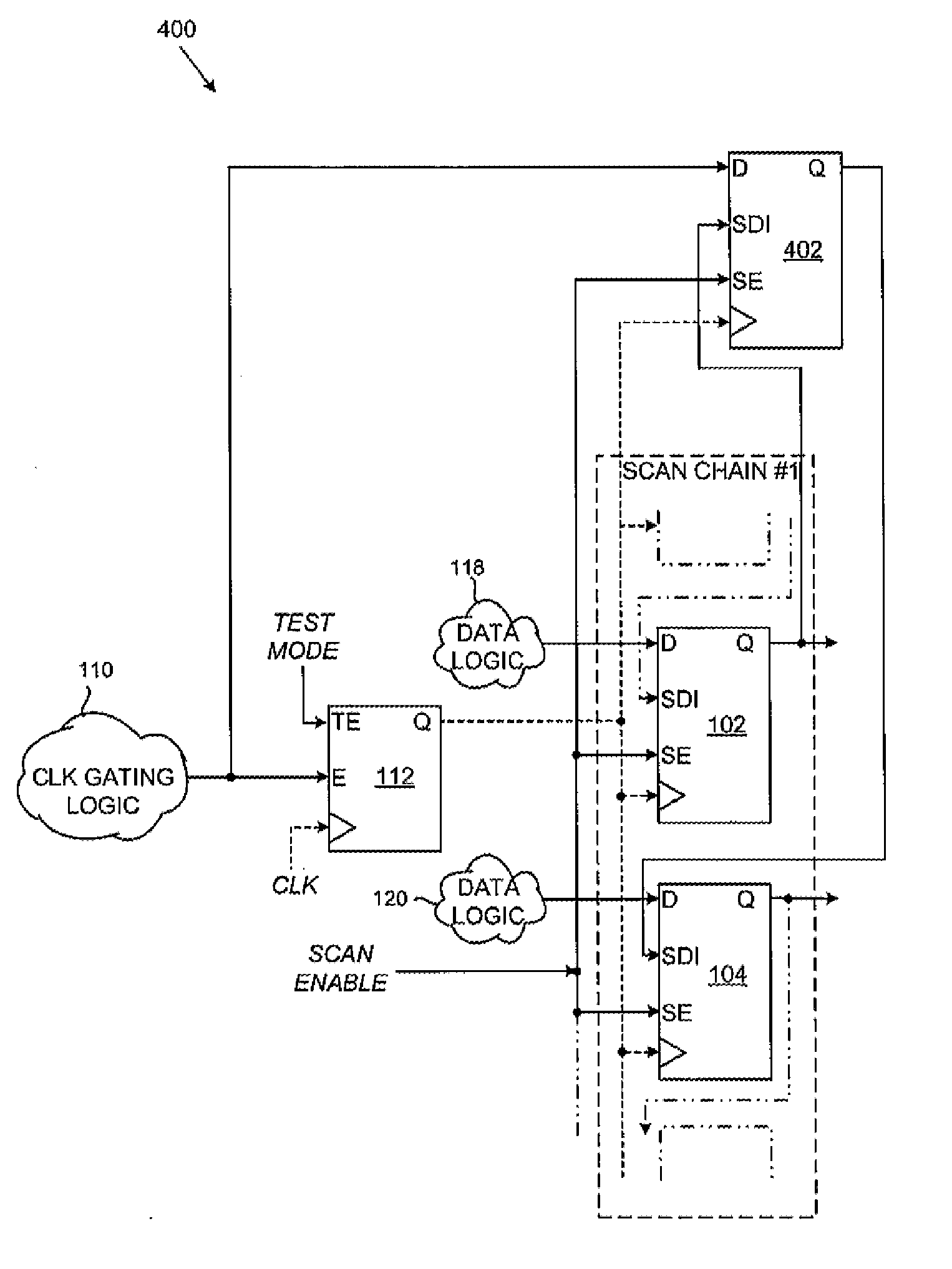
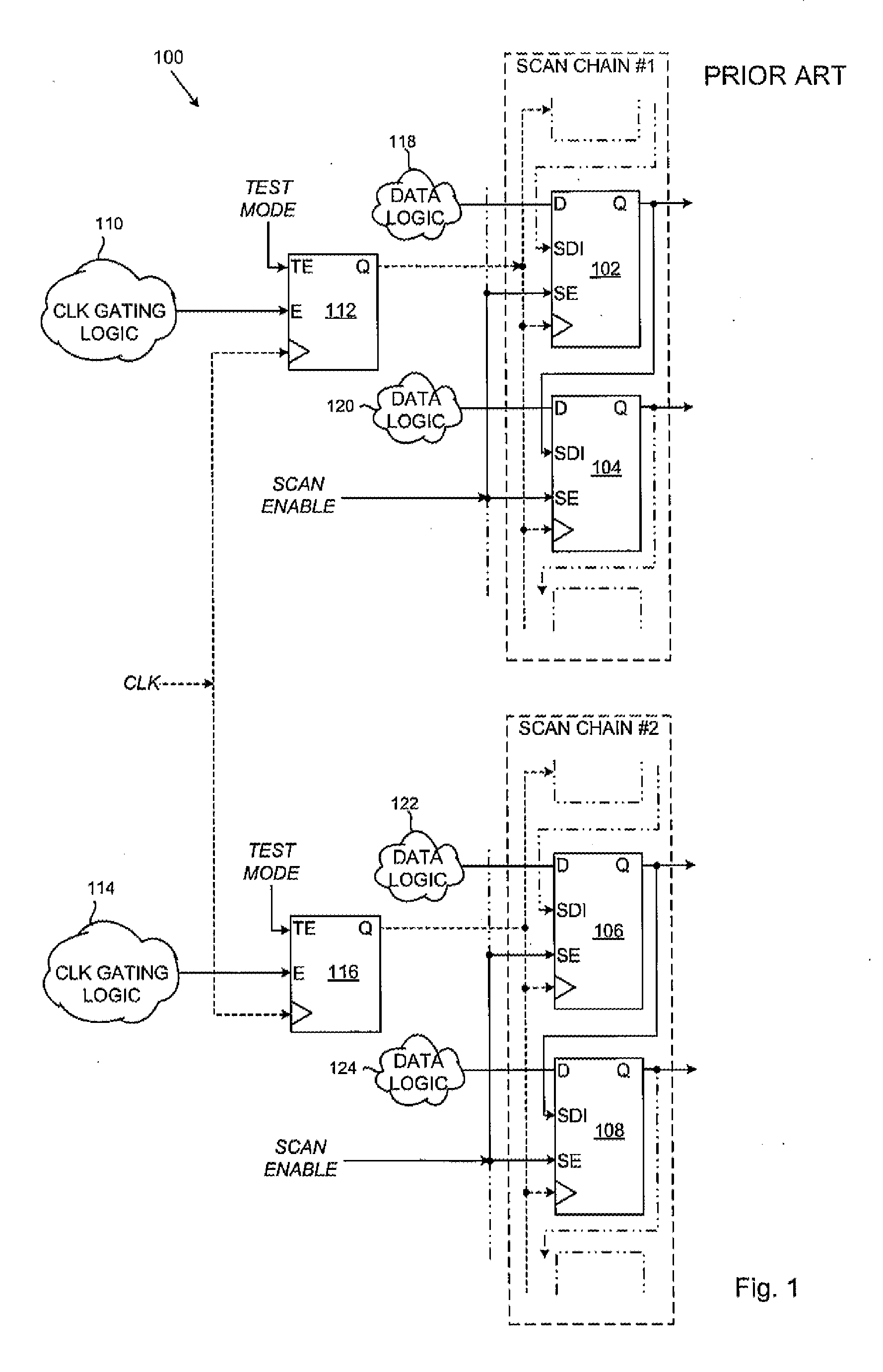
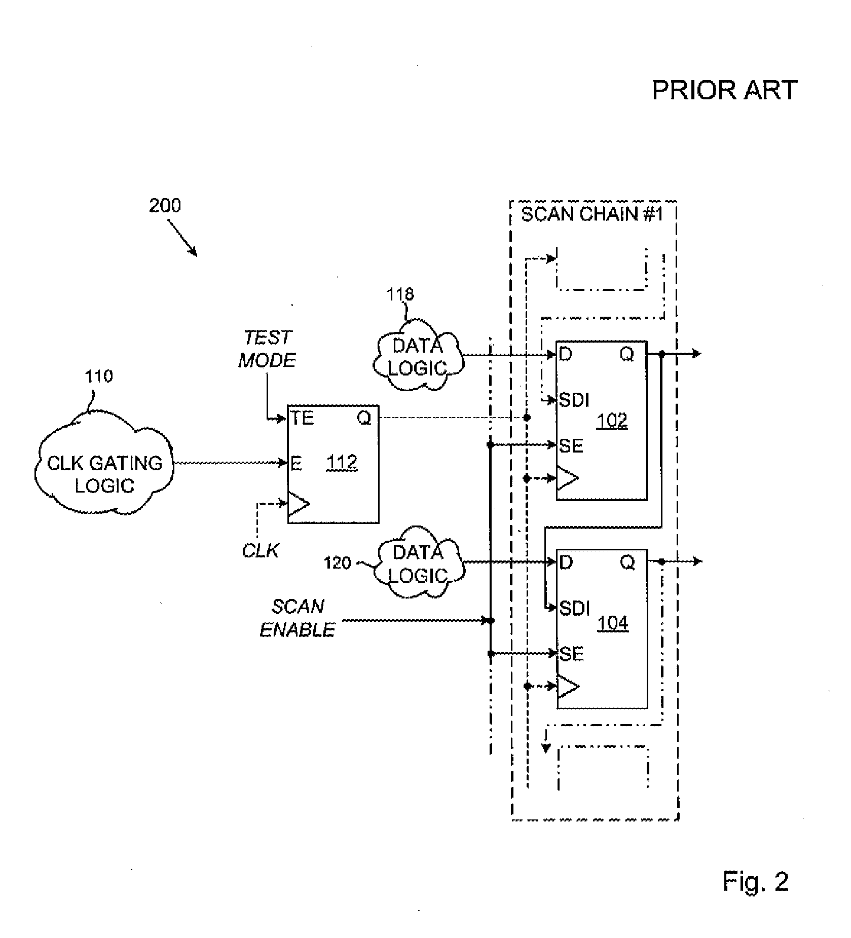
[0011]FIG. 1 illustrates an example of a typical electronic module 100 in an IC comprising output flip-flops such as 102, 104, 106 and 108, which can also be connected in a test scan chain. In this example, the flip-flops are connected in two separate scan chains SCAN CHAIN#1 and SCAN CHAIN#2. Each of the flip-flops 102-108 has a data input D, a data output Q, a scan data input SDI, a scan enable control input SE and a clock input. The SDI input of each of the flip-flops 102-108 is connected to the Q output of the previous flip-flop of the same scan chain, except for the first and last scan chain elements. The SDI input of the first scan chain element receives a test data input signal from a test access port (not shown). The output Q of the flip-flop of the last test scan chain element provides a test data output signal to the test access port. The flip-flops 102-108 receive from the test access port control signals TEST MODE and SCAN ENABLE.

[0012]The Q outputs of the flip-flops 102...


PUM


Abstract

An integrated circuit includes a set of cells for operation in a functional mode and in a scan testing mode, and a spare cell. The cells are connected in a scan chain with scan data inputs connected to the outputs of preceding cells in the scan chain and respond to assertion of a scan enable signal. A clock gating element applies a functional clock signal to clock inputs of the cells in response to a gating enable signal in functional mode and a test clock signal in response to a test mode signal in scan testing mode. A functional data input of the spare cell latches the gating enable signal during the scan testing mode in response to de-assertion of the scan enable signal. The output of the spare cell is connected to the scan data input of one of the cells in response to the scan enable signal.

Description

BACKGROUND OF THE INVENTION[0001]The present invention is directed to a method of scan testing clock gating cells of an integrated circuit, and to an integrated circuit having clock gating cells that can be scan tested.[0002]Dynamic power consumption of an integrated circuit (IC) can be reduced by techniques such as frequency and voltage scaling for the active modules of the IC, and by gating (turning OFF) the clock signals for inactive modules. Clock gating cells in the clock distribution network disable the inactive modules so that the flip-flops in the inactive modules do not switch states, as switching states consumes power. When not being switched, the dynamic switching power consumption goes to zero, and only leakage currents are incurred. Clock gating works by taking the functional enable conditions attached to the modules and using these enable conditions to gate the functional clocks.[0003]With the increase in complexity of IC devices, the complexity of testing these device...

Claims


Application Information

Patent Timeline
Patent Type & Authority Applications(United States)
IPC IPC(8): G01R31/28G06F11/22
CPCG01R31/318552G01R31/318541
Inventor KUKREJA, HIMANSHUAGRAWAL, DEEPAK
Owner FREESCALE SEMICON INC
Why Eureka
Try Eureka