
High efficiency light emitting diode

a light-emitting diode, high-efficiency technology, applied in the direction of basic electric elements, electrical apparatus, semiconductor devices, etc., can solve the problems of sapphire substrate light-emitting efficiency decline, sapphire substrate light-emitting efficiency reduction, and light-emitting portion, etc., to maximize the internal reflecting improve the light-emitting efficiency of the substrate, and minimize the amount of light absorbed

Inactive Publication Date: 2013-05-23
SEOUL VIOSYS CO LTD
View PDF15 Cites 6 Cited by
  • Summary
  • Abstract
  • Description
  • Claims
  • Application Information

AI Technical Summary

Benefits of technology

The present invention provides a high-efficiency LED that can minimize the amount of light that is absorbed by the electrode pad and the light that is not emitted to the outside of the LED. This is achieved by forming light-reflecting structures on both the substrate and electrode pad to maximize the internal reflecting efficiency of the substrate and minimize the amount of light that does not escape to the outside. This results in a more efficient LED with improved light-emitting efficiency.

Problems solved by technology

However, since the blue LED is typically grown over an insulating sapphire substrate, both an n-electrode and a p-electrode are disposed on the same side (over a nitride semiconductor that is produced by crystal growth) unlike existing LEDs using a conductive substrate, and thus its drawback is a reduced light-emitting area.
However, the LED of the related art has a problem in that a portion of light, which was emitted from the active layer and entered the sapphire substrate, is trapped inside the sapphire substrate due to inferior reflecting efficiency.
This not only worsens the light-emitting efficiency of the LED, but also generates heat.
However, this structure has a problem of limited light extraction efficiency.

Method used


Image

  • High efficiency light emitting diode
  • High efficiency light emitting diode
  • High efficiency light emitting diode

Examples


Embodiment Construction

[0034]The present invention will now be described more fully hereinafter with reference to the accompanying drawings, in which exemplary embodiments thereof are shown, so that this disclosure will fully convey the scope of the present invention to those skilled in the art. This invention can, however, be embodied in many different forms and should not be construed to be limited to the embodiments set forth herein.

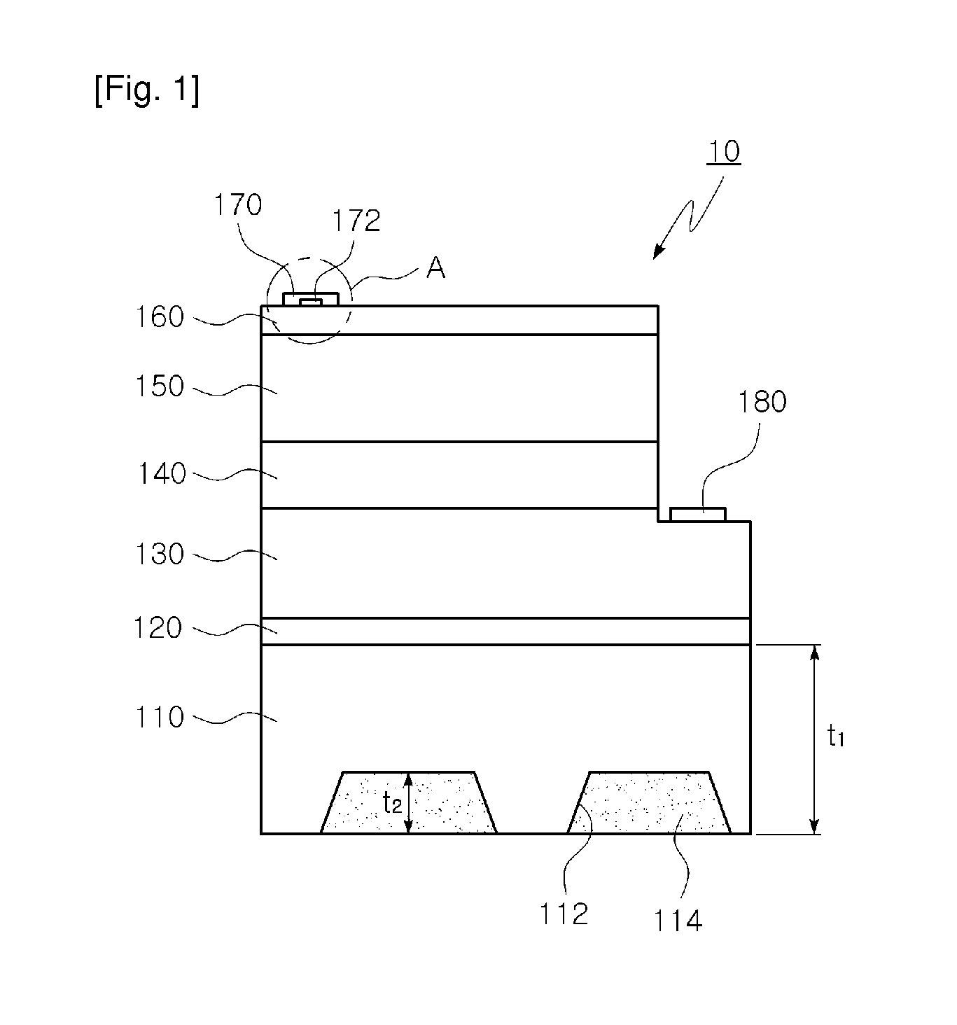
[0035]First, a high-efficiency Light-Emitting Diode (LED) according to an exemplary embodiment of the invention is described with reference to FIG. 1.

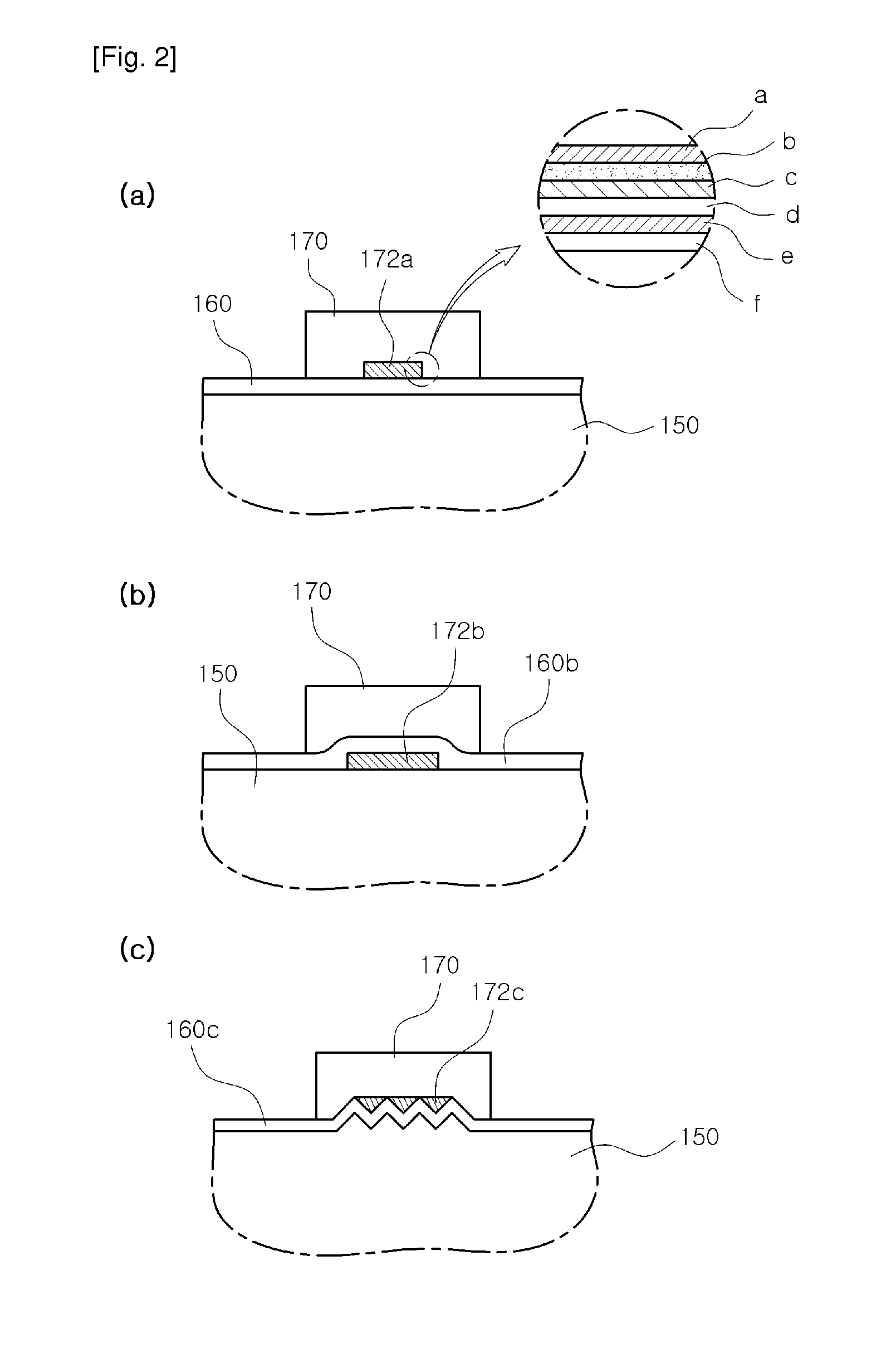
[0036]FIG. 1 is a cross-sectional view showing a high-efficiency LED according to an exemplary embodiment of the invention, FIG. 2 is an enlarged cross-sectional view of part A of FIG. 1 in which an electrode pad is formed, and FIG. 3 is a top plan view of the high-efficiency LED shown in FIG. 1.

[0037]As shown in FIG. 1, an LED 10 includes a substrate 110, which has recesses 112 in the underside thereof. A buffer layer 120 is ...


PUM


Abstract

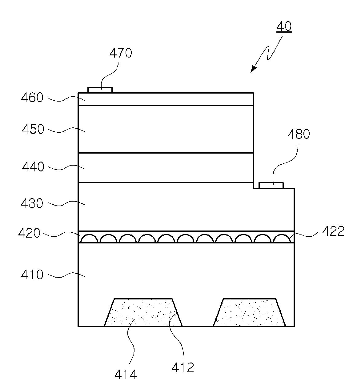
A high-efficiency LED includes a substrate, an n-semiconductor layer, an active layer, a p-semiconductor layer, and a transparent electrode layer. The substrate has a plurality of tapered recesses in the underside thereof, the recesses being filled with light-reflecting filler.

Description

CROSS-REFERENCE TO RELATED APPLICATIONS[0001]This application is the National Stage Entry of International Application No. PCT / KR2010 / 008560, filed on Dec. 1, 2010, and claims priority from and the benefit of Korean Patent Application No. 10-2010-0092848, filed on Sep. 24, 2010, both of which are hereby incorporated by reference for all purposes as if fully set forth hereinBACKGROUND[0002]1. Field[0003]The present invention relates to a high-efficiency Light-Emitting Diode (LED), and more particularly, to a high-efficiency LED, which can have a light-reflecting structure to improve the internal reflecting efficiency of a substrate and minimize the amount of light absorbed by an electrode pad, thereby improving light-emitting efficiency.[0004]2. Discussion of the Background[0005]Since the development of a nitride semiconductor light-emitting device (e.g., an LED, a laser diode, or the like made of group III nitride-based compound semiconductor), it has been gaining attention as a maj...

Claims


Application Information

Patent Timeline
Patent Type & Authority Applications(United States)
IPC IPC(8): H01L33/10
CPCH01L33/20H01L33/38H01L33/0079H01L2933/0091H01L33/10H01L33/46H01L33/405H01L33/0093
Inventor YOON, YEO JINSEO, WON CHEOL
Owner SEOUL VIOSYS CO LTD
Learn More