
Highly reflective coating on LED submount

a submount and reflective technology, applied in the direction of semiconductor/solid-state device manufacturing, semiconductor devices, electrical apparatus, etc., can solve the problems of reducing the loss of efficiency caused by the loss of efficiency, the inability to use a reflector cup generally economically viable, and the inability to achieve the effect of enhancing luminance output, minimizing light loss and/or absorption, and enhancing luminance outpu

Active Publication Date: 2013-09-26
LUMILEDS
View PDF6 Cites 3 Cited by
  • Summary
  • Abstract
  • Description
  • Claims
  • Application Information

AI Technical Summary

Benefits of technology

The patent text is about a new method for improving the efficiency of light emitting devices. The method involves adding a highly reflective coating to the substrate that supports the device. This helps to reduce light loss and absorption through the substrate and increases the amount of light that reaches the desired output. The method also includes using a submount with a metallization layer and a planar dielectric layer to further minimize light loss. Additionally, pedestal elements are added to facilitate the coupling of the device's components. This patent aims to provide a better way to produce light emitting devices with enhanced luminance output.

Problems solved by technology

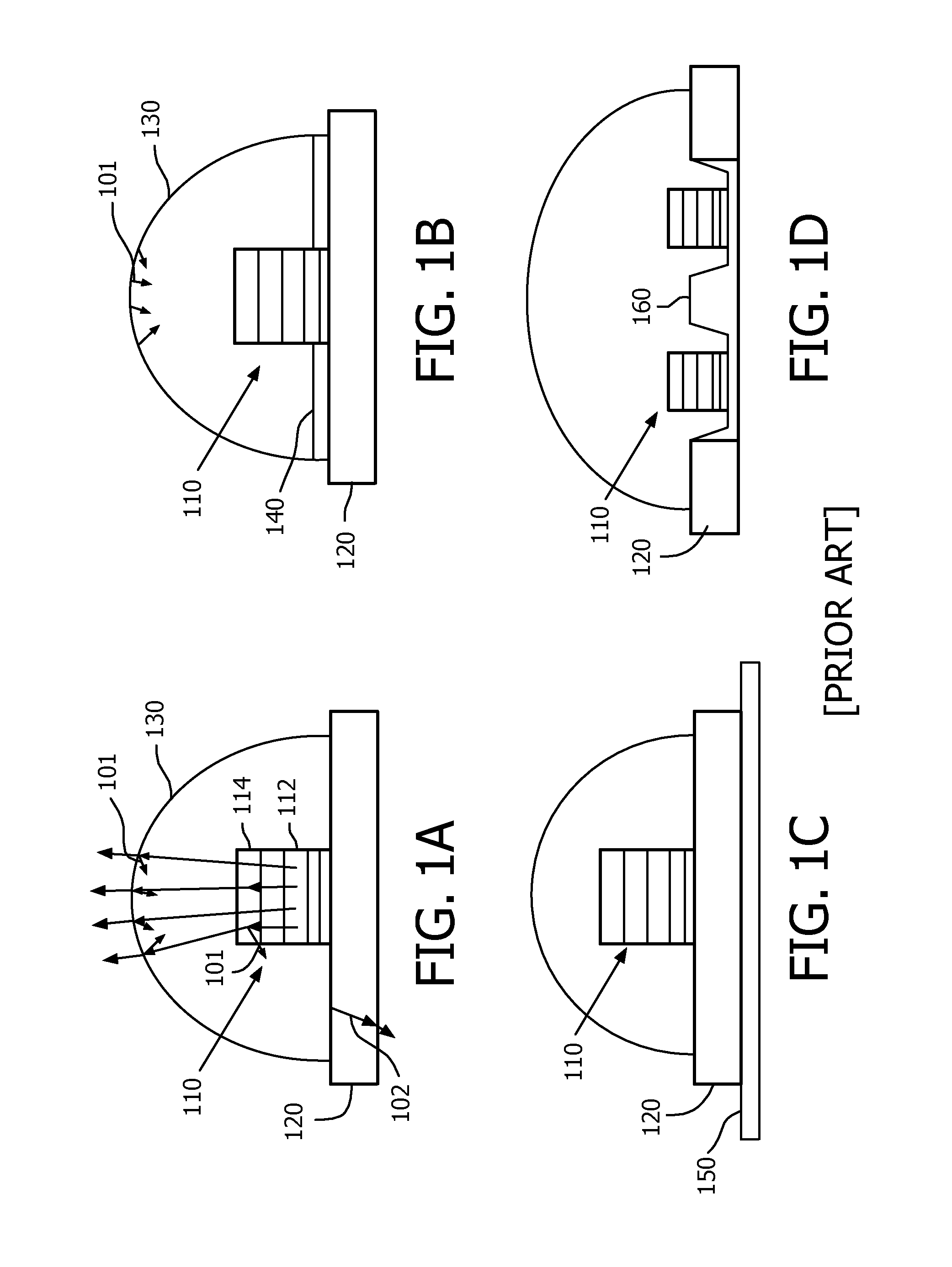
Although most of the emitted and converted light is output from the optical element 130, some of the light 101 is internally reflected or otherwise misdirected, resulting in a loss of efficiency.
However, with the advent of die on ceramic (DoC) LED packaging, the use of a reflector cup is not generally economically viable.
In this manner, the internally reflected light 101 is reflected back up to the lens element 130, thereby potentially reducing the loss of efficiency caused by this internally reflected light 101.
However, this arrangement does not allow the stack 110 to be mounted on the substrate 120.

Method used


Image

  • Highly reflective coating on LED submount
  • Highly reflective coating on LED submount
  • Highly reflective coating on LED submount

Examples


Embodiment Construction

[0019]In the following description, for purposes of explanation rather than limitation, specific details are set forth such as the particular architecture, interfaces, techniques, etc., in order to provide a thorough understanding of the concepts of the invention. However, it will be apparent to those skilled in the art that the present invention may be practiced in other embodiments, which depart from these specific details. In like manner, the text of this description is directed to the example embodiments as illustrated in the Figures, and is not intended to limit the claimed invention beyond the limits expressly included in the claims. For purposes of simplicity and clarity, detailed descriptions of well-known devices, circuits, and methods are omitted so as not to obscure the description of the present invention with unnecessary detail.

[0020]Copending U.S. patent application Ser. No. 12 / 508,238, “LED WITH MOLDED REFLECTIVE SIDEWALL COATING” filed 23 Jul. 2009 for Serge Bierhuiz...


PUM


Abstract

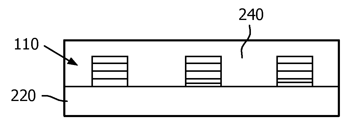
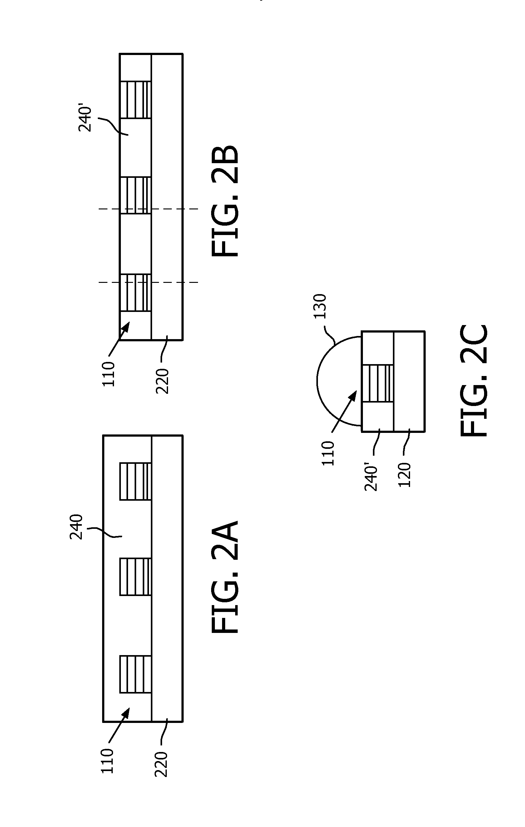
A submount for a light emitting stack includes a substrate and a metallization layer having circuit traces and a planar dielectric layer that fills regions between the circuit traces. The planar dielectric layer serves to minimize the amount of light lost / absorbed by the substrate and preferably reflects the internally reflected light back toward the desired light output element. To facilitate efficient manufacture, a dielectric paste is applied over the metallized layer, then planed to expose at least portions of the metal conductors for the subsequent coupling to the light emitting stack. Pedestal elements are preferably provided at select locations on the circuit traces to facilitate this coupling while allowing the remainder of the circuit traces to be covered with the dielectric layer.

Description

BACKGROUND AND SUMMARY OF THE INVENTION[0001]This invention relates to the field of light emitting devices, and in particular to a light emitting device with improved efficiency by providing a highly reflective coating on the substrate that supports the light emitting device.[0002]The need for energy efficient illumination has accelerated the demand for efficient light emitting devices, particularly in view of the fact that solid state light emitting devices are now able to provide white light by mixing light of multiple wavelengths.[0003]In a typical solid state multiple wavelength light emitting device, an active element of a light emitting structure provides light of a first wavelength, and a wavelength conversion element converts some of this light into light of a second wavelength. The wavelengths provided by the light of the light emitting element and the wavelength conversion elements, and the proportions of each, are designed / selected so as to produce a desired combination o...

Claims


Application Information

Patent Timeline
Patent Type & Authority Applications(United States)
IPC IPC(8): H01L33/60H01L33/50
CPCH01L33/60H01L33/62H01L33/50H01L2924/0002H01L2924/00H01L2933/0066H01L33/48
Inventor MORAN, BRENDANKMETEC, JEFFREYBLACK, IAINDIANA, FREDERICRUDAZ, SERGE LAURENTZHANG, LI
Owner LUMILEDS
Learn More