Display panel for display device and method for detecting defects of signal lines for display devices

a display device and display panel technology, applied in the field of display devices, can solve the problems of difficult detection of whether, precise location of shorted and/or opened signal lines, and inability to determine whether, so as to increase the resistance between adjacent signal lines and eliminate signal interference

Active Publication Date: 2013-05-30
LG DISPLAY CO LTD
View PDF7 Cites 24 Cited by
  • Summary
  • Abstract
  • Description
  • Claims
  • Application Information

AI Technical Summary

Benefits of technology

[0009]Embodiments include a display panel for display devices having a structure of signal lines that allows adjacent signal lines to have different electrical connection methods, and thus increases the difference in resistance between the adjacent signal lines and eliminates signal interference between the adjacent signal lines. Beneficially, it is possible to precisely determine whether or not the respective signal lines are shorted and whether or not the plurality of signal lines are opened. Embodiments also include a method for detecting defects of signal lines for display devices having such structure.

Problems solved by technology

Thereby, the space between signal lines is inevitably reduced.
Therefore, in conventional display devices, signal waveforms detected from adjacent signal lines are almost similar due to signal interference between the adjacent signal lines, and thus detection as to whether or not the respective signal lines are shorted and / or opened and the precise location of the shorted and / or opened signal lines may be difficult to determine.

Method used


Image

  • Display panel for display device and method for detecting defects of signal lines for display devices
  • Display panel for display device and method for detecting defects of signal lines for display devices
  • Display panel for display device and method for detecting defects of signal lines for display devices

Examples


first embodiment

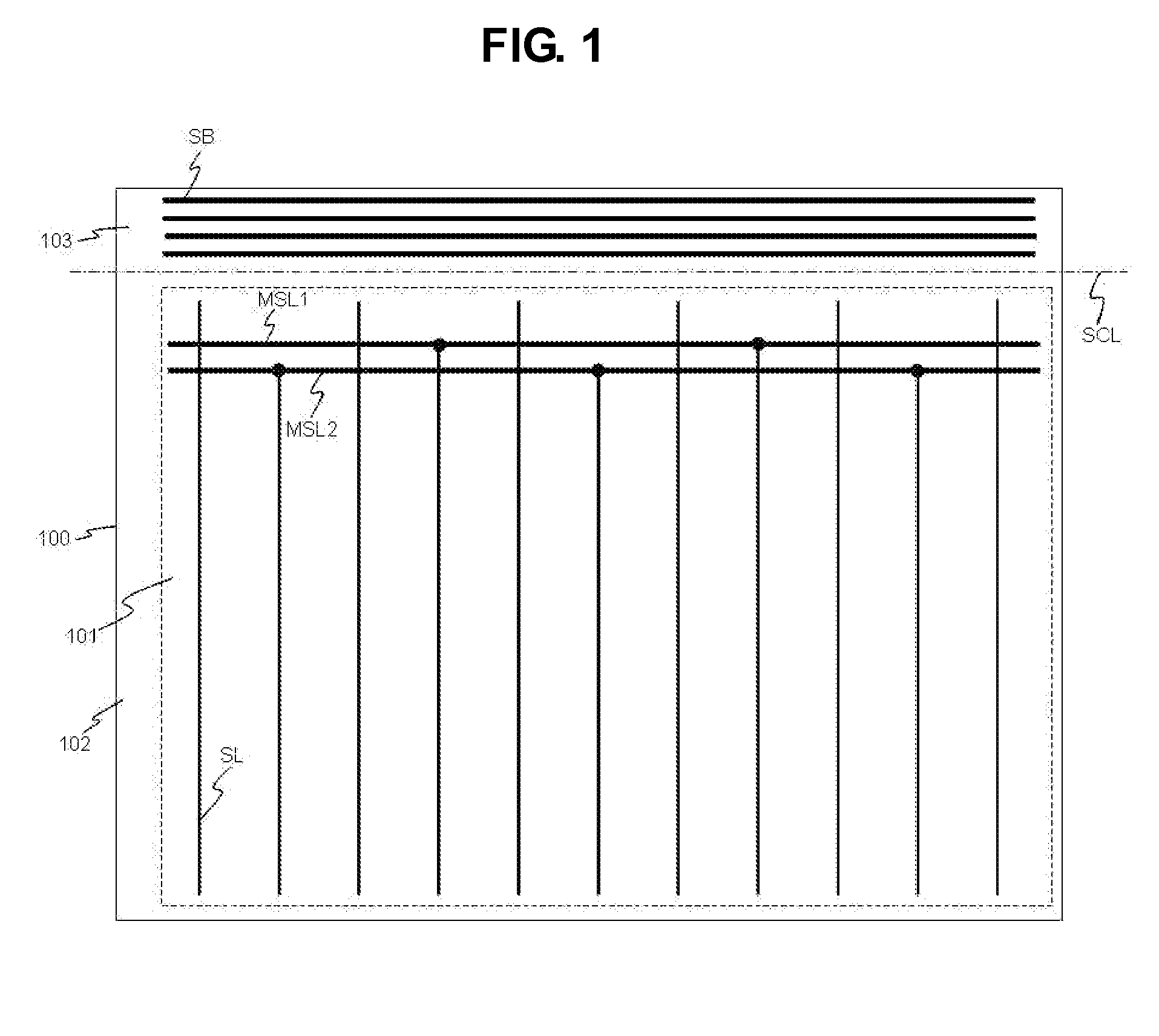
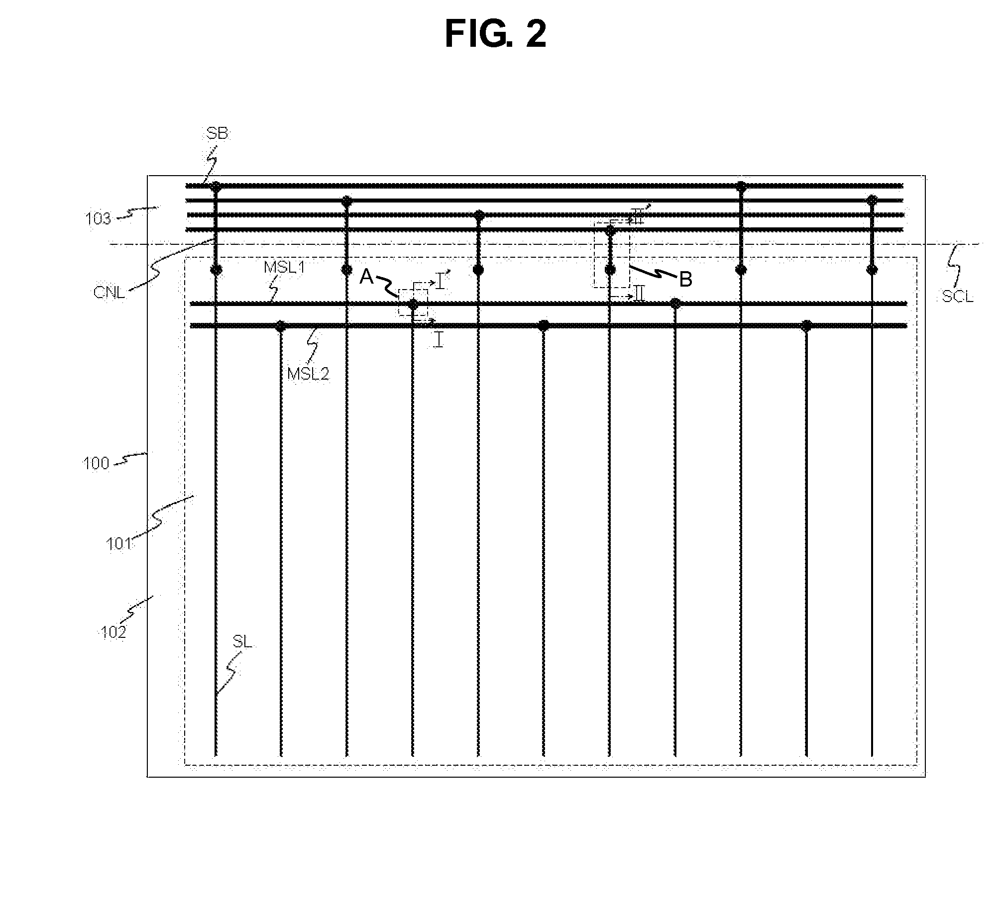
[0046]FIG. 1 illustrates a display panel for display devices in accordance with the present invention.

[0047]The display panel for display devices in accordance with the first embodiment of the present invention, as shown in FIG. 1, includes a substrate 100 on which a plurality of signal lines SL to transmit various signals required by pixels is formed.

[0048]The substrate 100 is divided into a display area 101, a non-display area 102 and a shorting bar area 103. The substrate 100 shown in FIG. 1 is a lower substrate from among two substrates of the display panel, and FIG. 1 does not illustrate an upper substrate. The shorting bar area 103 is removed from the substrate 100 after a final test. For example, the shorting bar area 103 is removed from the substrate 100 by cutting the substrate 100 along a scribing line SCL of FIG. 1.

[0049]The pixels and the signal lines SL are formed in the display area 101, as described above. Further, first and second main signal transmission lines MSL1 ...

second embodiment

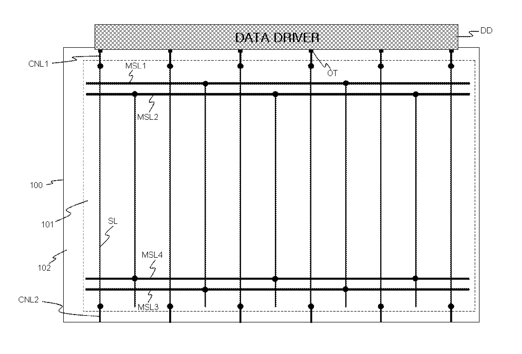
[0094]FIG. 8 illustrates a display panel for display devices in accordance with the present invention.

[0095]The display panel for display devices in accordance with the second embodiment of the present invention, as shown in FIG. 8, includes a substrate 100 on which a plurality of signal lines SL to transmit various signals required by pixels is formed.

[0096]The substrate 100 is divided into a display area 101, a non-display area 102, a first shorting bar area 103 and a second shorting bar area 104. The substrate 100 shown in FIG. 8 is a lower substrate from among two substrates of the display panel, and FIG. 8 does not illustrate an upper substrate.

[0097]The pixels and the signal lines SL are formed in the display area 101, as described above. Further, first to fourth main signal transmission lines MSL1 to MSL4 are formed in the display area 101. Alternatively, the first to fourth main signal transmission lines MSL1 to MSL4 may be formed in the non-display area 102 rather than the ...


PUM


Abstract

A display panel for display devices which enables precisely determining whether or not adjacent signal lines are shorted or opened and a method for detecting defects of the signal lines are disclosed. The display panel includes a substrate on which a plurality of signal lines to transmit various signals required by pixels is formed, and one of any two adjacent signal lines is connected to at least one of main signal transmission lines and the other one of the two adjacent signal lines is maintained in a floating state.

Description

CROSS-REFERENCE TO RELATED APPLICATIONS[0001]This application claims priority under 35 U.S.C. §119(a) from Republic of Korea Patent Application No. 10-2011-0124437 filed on Nov. 25, 2011 and from Republic of Korea Patent Application No. 10-2012-0044758 filed on Apr. 27, 2012, which is hereby incorporated by reference as if fully set forth herein.BACKGROUND OF THE INVENTION[0002]1. Field of the Invention[0003]The present invention relates to a display device, and more particularly, to a display panel for display devices which precisely determines whether or not adjacent signal lines are shorted and / or opened and a method for detecting defects of signal lines for display devices.[0004]2. Discussion of the Related Art[0005]Display devices, such as a liquid crystal display device, a plasma display device and a light emitting display device, generally go through several test processes before they are put on the market.[0006]These various processes include a process of testing short and o...

Claims


Application Information

Patent Timeline
Patent Type & Authority Applications(United States)
IPC IPC(8): G01R31/02G09G5/00
CPCG09G3/006G09G3/3233G09G3/20
Inventor YUN, SOON-ILOH, DU-HWAN
Owner LG DISPLAY CO LTD
Why Eureka
Try Eureka