Touch panel having border without color difference and manufacturing method thereof

a technology of color difference and touch panel, applied in the field of input panel, can solve the problem of reducing the space provided by the housing for assembling the border, and achieve the effect of avoiding the exposedness of the border circuit, improving functions, and reducing the number of additional attaching or assembly steps to achieve the desired decoration purpos

Inactive Publication Date: 2013-05-30
WISTRON CORP
View PDF13 Cites 31 Cited by
  • Summary
  • Abstract
  • Description
  • Claims
  • Application Information

AI Technical Summary

Benefits of technology

[0023]As mentioned above, the present invention configures the transparent conductive connecting layer extending from the transparent conductive layer to the shielding decoration layer and exceeding the edge of the transparent conductive layer. Moreover, the opaque conductive layer is disposed on the transparent conductive connecting layer and is not disposed on the transparent conductive layer. This configuration can effectively avoid the exposedness of the border circuit, so that the user can not view the border circuit. Besides, only a single substrate is used in the touch panel and its manufacturing method of the invention, so that the additional transparent adhesive or cover lens is unnecessary, which can make the products become thinner.
[0024]More advantageously, the substrate of the touch panel of the present invention has multiple functions, which is not available in the conventional art. The multiple functions include: a decoration function for decorating and shielding the internal circuits, a protection function for protecting the conductive layer and the internal circuits, and a complete touch control function provided by configuring the complete conductive layer. In brief, the conventional art needs additional manufacturing processes and materials to form a cover for providing the desired decoration and protection functions; on the contrary, the novel design of this invention can easily carry out the concept of multi-function substrate. Since the substrate of this invention has improved functions, it is possible to omit another substrate in the panel. Thus, the additional attaching or assembling steps for providing the desired decoration purpose can be reduced, so the invention is suitable for modulation processes and can decrease the manufacturing cost.

Problems solved by technology

Although the border can cover and block the inaesthetic part, such as the insulation layer and the flexible printed circuit board pattern, an additional drawback that the housing must provide some extra spaces for assembling the border occurs.

Method used


Image

  • Touch panel having border without color difference and manufacturing method thereof
  • Touch panel having border without color difference and manufacturing method thereof
  • Touch panel having border without color difference and manufacturing method thereof

Examples


Embodiment Construction

[0029]The present invention will be apparent from the following detailed description, which proceeds with reference to the accompanying drawings, wherein the same references relate to the same elements.

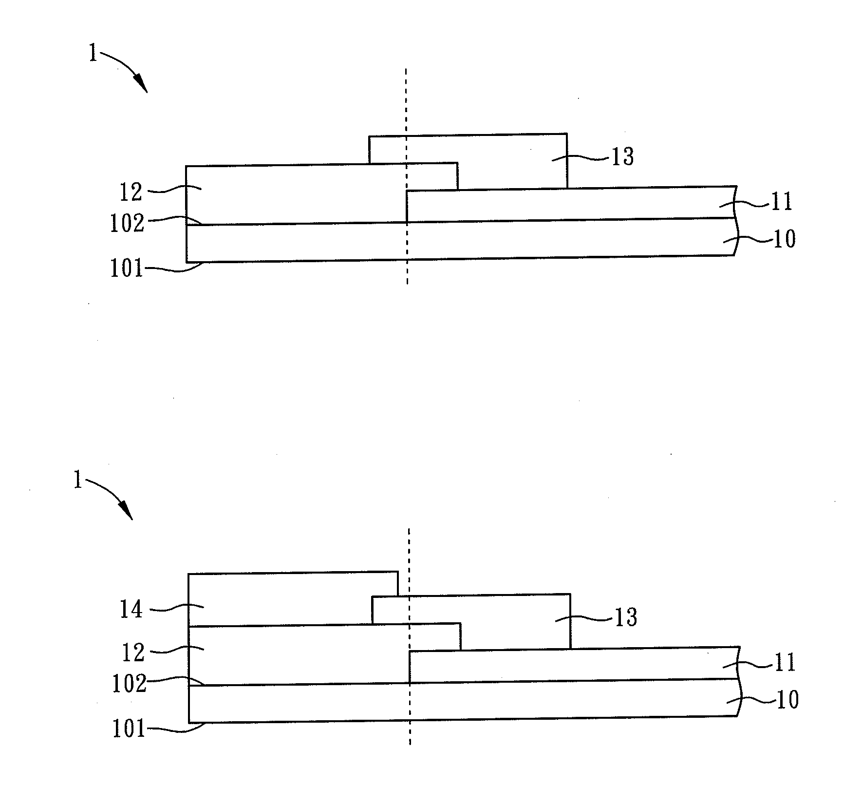
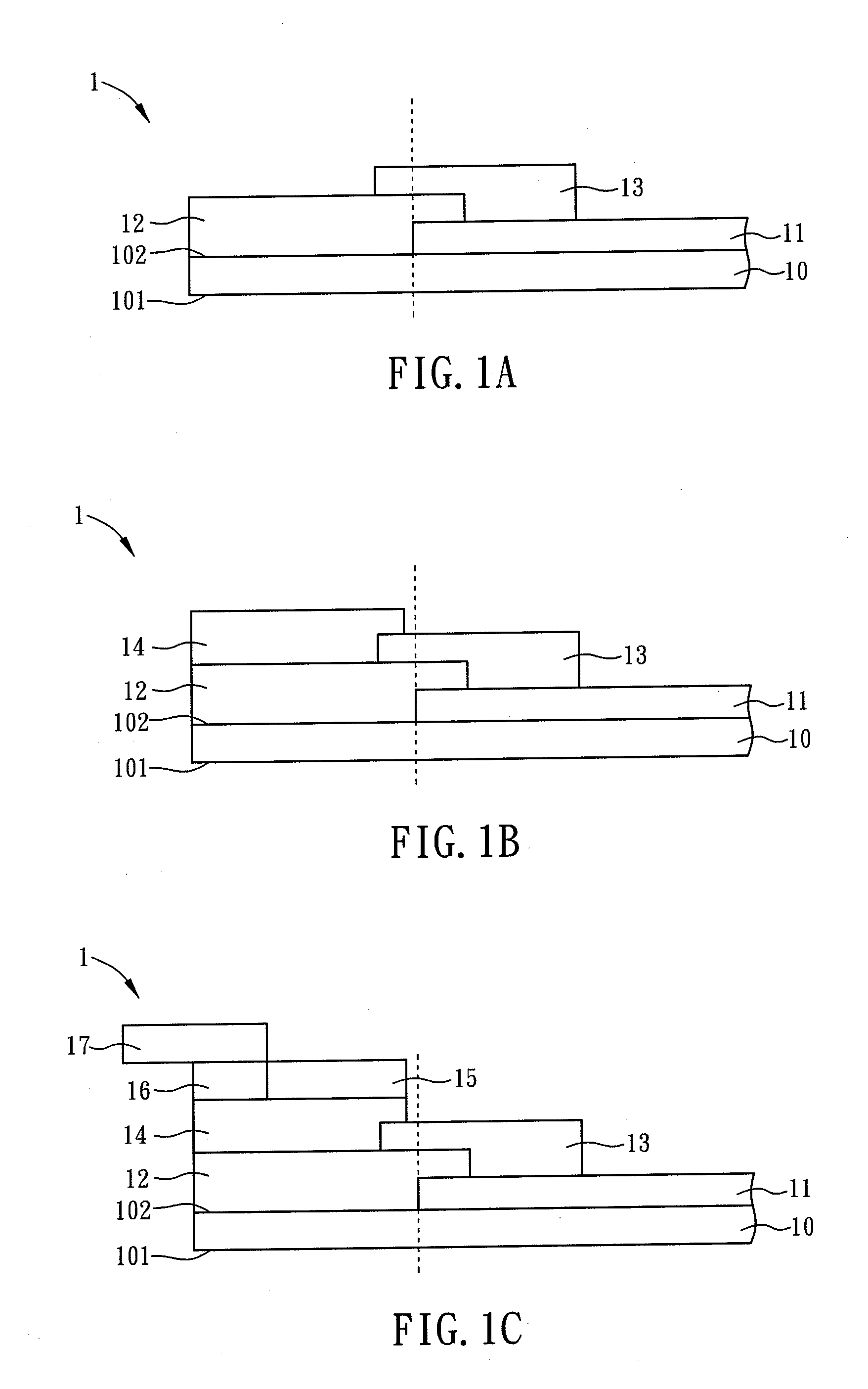
[0030]FIGS. 1A to 1C are schematic diagrams of a touch panel 1 of a preferred embodiment of the present invention. As shown in FIG. 1A, the touch panel 1 includes a substrate 10, a transparent conductive layer 11, a shielding decoration layer 12 and a transparent conductive connecting layer 13. The transparent conductive layer 11 is disposed on the substrate 10, and the shielding decoration layer 12 is disposed on the substrate 10 and the transparent conductive layer 11.

[0031]For example, the transparent conductive layer 11, the shielding decoration layer 12 and the transparent conductive connecting layer 13 can be formed on the substrate 10 by the following steps of: forming the transparent conductive layer 11 on the substrate 10; forming the shielding decoration layer 12 on the subs...


PUM

PropertyMeasurementUnit
transparent conductiveaaaaaaaaaa
transparentaaaaaaaaaa
conductiveaaaaaaaaaa

Abstract

A touch panel includes a substrate, a transparent conductive layer, a shielding decoration layer, a transparent conductive connecting layer and an opaque conductive layer. The transparent conductive layer is disposed on the substrate. The shielding decoration layer is disposed on the substrate and the transparent conductive layer. The transparent conductive connecting layer is disposed on the transparent conductive layer and the shielding decoration layer, extends from the transparent conductive layer to the shielding decoration layer, and exceeds an edge of the transparent conductive layer. The opaque conductive layer is disposed on the shielding decoration layer and the transparent conductive connecting layer, and is not disposed on the transparent conductive layer.

Description

CROSS REFERENCE TO RELATED APPLICATIONS[0001]This Non-provisional application claims priority under 35 U.S.C. §119(a) on Patent Application No(s). 100143443 filed in Taiwan, Republic of China on Nov. 25, 2011, the entire contents of which are hereby incorporated by reference.BACKGROUND OF THE INVENTION[0002]1. Field of Invention[0003]The invention relates to an input panel and a manufacturing method thereof and, in particular, to a touch panel and a manufacturing method thereof.[0004]2. Related Art[0005]Various kinds of touch input devices have been widely applied to many electronic products, such as mobile phones and tablet computers are mostly configured with a touch panel as their input device. A user can simply use his hand to touch a surface of the touch panel directly to input a command, or move his hand on the surface to control a cursor or input words by writing. Besides, the display panel cooperated with the touch panel can show virtual buttons, so that the user can click t...

Claims


Application Information

Patent Timeline
Patent Type & Authority Applications(United States)
IPC IPC(8): G06F3/041H01H49/00
CPCG06F3/041Y10T29/49105G06F2203/04103H01H49/00G06F3/04164G06F3/044G06F2203/04107
Inventor WANG, KUEI-CHINGLIN, TA-HU
Owner WISTRON CORP
Why Eureka
Try Eureka