Structure and production process of a microelectronic 3D memory device of flash NAND type

Active Publication Date: 2011-07-14
COMMISSARIAT A LENERGIE ATOMIQUE ET AUX ENERGIES ALTERNATIVES
View PDF8 Cites 72 Cited by
  • Summary
  • Abstract
  • Description
  • Claims
  • Application Information

AI Technical Summary

Benefits of technology

[0029]This guarantees good quality of the gate tunnel dielectrical and good interface quality between the channels and the dielectrical tunnel relative to a deposited oxide.
[0030]The fir

Problems solved by technology

For memory technologies in which the gate lengths are less than 30 nm, memory performance is limited due to insufficient insulation of memory points from one another, and the effects of short channels.
Also, lithographic processes for critical dimensions below 30 nanometres present difficulties in execution.
The latter can boost production costs significantly.
However, due to the production process of the second active semi-conductor layer 2, the channels of the tra

Method used


Image

  • Structure and production process of a microelectronic 3D memory device of flash NAND type
  • Structure and production process of a microelectronic 3D memory device of flash NAND type
  • Structure and production process of a microelectronic 3D memory device of flash NAND type

Examples


Embodiment Construction

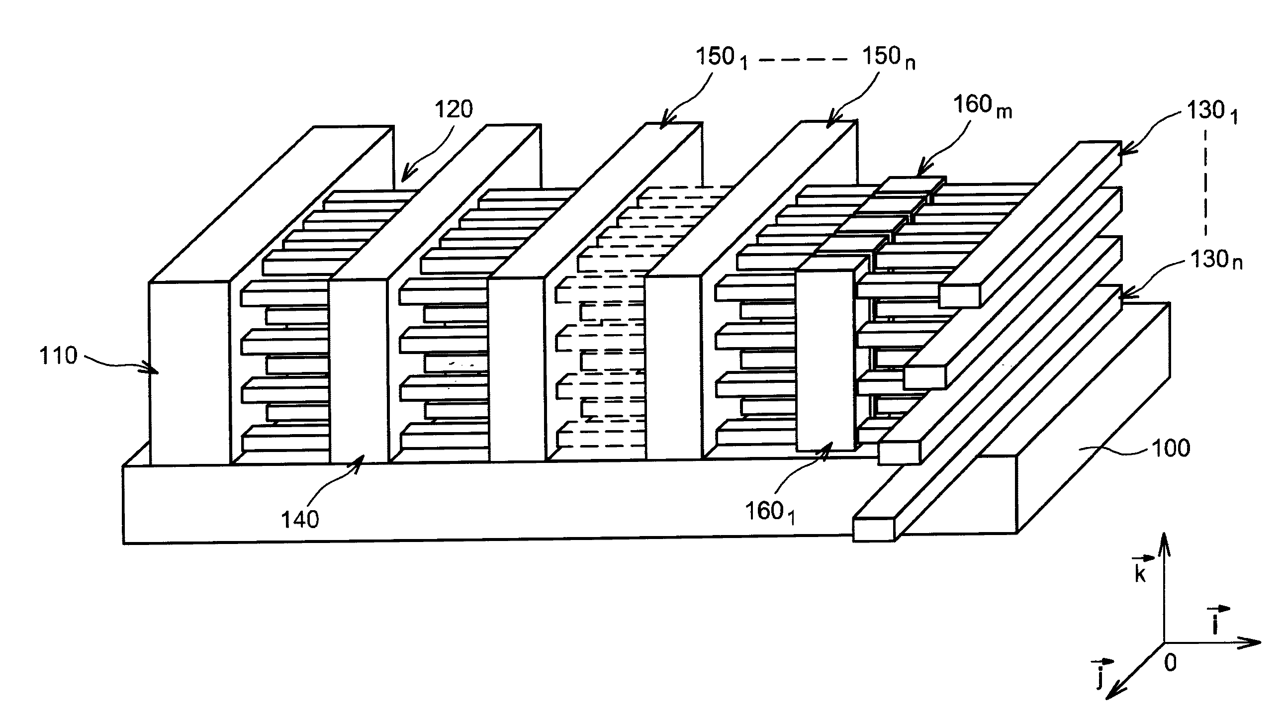
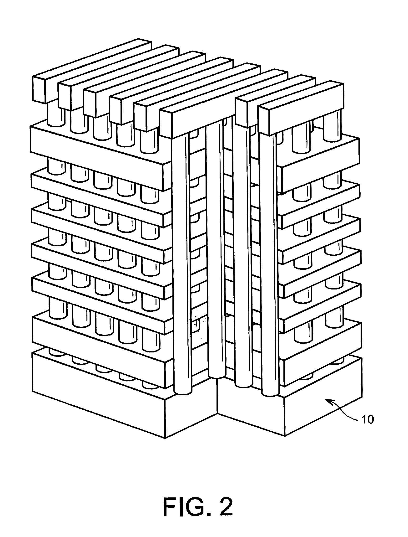
[0085]An example of a device microelectronic of memory three-dimensional will now be described in conjunction with FIG. 3.

[0086]This memory can comprise m*n*p memory points or memory cells and can be of Flash type, that is, rewritable semi-conductor memory having the characteristics of live memory, but whereof the data do not vanish when turned off.

[0087]So, the flash memory stores one bit or bits of data in memory cells, these data being kept in memory when the power supply of the memory is cut.

[0088]The memory can have architecture similar to that of flash memory of NAND type.

[0089]FLASH memories of NAND type are accessible by block and offer very strong density of memory points per surface unit to the extent where they need few interconnections.

[0090]The device first comprises a substrate 100 which can be of semi-conductor on insulator type, for example of SOI (SOI for “Silicon On Insulator”) type or can be a solid semi-conductor substrate (“bulk”).

[0091]The substrate 100 acts as...


PUM


Abstract

A microelectronic flash memory device including a plurality of memory cells including transistors fitted with a matrix of channels connecting a block of common source to a second block on which bit lines rest, the transistors also being formed by a plurality of gates including at least one gate material, including a first selection gate coating the channels, a plurality of control gates coating the channels, a plurality of second selection gates each coating the channels of the same row and the matricial arrangement, at least one or more of the gates based on superposition of layers including at least one first layer of dielectrical material, at least one charge store zone, and at least one second layer of dielectrical material.

Description

TECHNICAL FIELD[0001]The present invention relates to the field of microelectronics, and more particularly to that of memories, and its aim is to provide rewritable 3D memory, in particular non-volatile memory of Flash type, such as NAND memory, comprising memory points or cells distributed in 3 dimensions, formed by means of at least one structure comprising several gates formed about bars based on parallel semi-conductor material connecting semi-conductor blocks, the gates based on superposition of layers comprising at least one charge storage zone.[0002]The present invention also relates to a production process of such memory.PRIOR ART[0003]Continuing efforts are being made to increase the density of memories. For this, an attempt is made to make cells increasingly smaller in size. For memory technologies in which the gate lengths are less than 30 nm, memory performance is limited due to insufficient insulation of memory points from one another, and the effects of short channels....

Claims


Application Information

Patent Timeline
IPC IPC(8): H01L29/788H01L21/336
CPCH01L21/8221H01L27/0688H01L27/115H01L27/1203H01L27/11578H01L27/11582H01L27/11568H10B69/00H10B43/20H10B43/30H10B43/27
Inventor ERNST, THOMASMOLAS, GABRIELDE SALVO, BARBARABECU, STEPHANE
Owner COMMISSARIAT A LENERGIE ATOMIQUE ET AUX ENERGIES ALTERNATIVES
Why Eureka
Try Eureka