Manufacturing method of dielectric layer

A manufacturing method and dielectric layer technology, applied in semiconductor/solid-state device manufacturing, circuits, electrical components, etc., can solve problems such as capacitor performance deterioration, large leakage current, and complicated process steps, so as to reduce defects, prevent leakage, and The effect of simplifying the process

Inactive Publication Date: 2004-03-31
PROMOS TECH INC
View PDF0 Cites 8 Cited by
  • Summary
  • Abstract
  • Description
  • Claims
  • Application Information

AI Technical Summary

Problems solved by technology

However, the silicon nitride / silicon oxide / silicon nitride (NON) stacked dielectric layer has a large leakage current, and the process of making this silicon nitride / silicon oxide / silicon nitride (NON) stacked dielectric layer The steps are more complicated
[0007] For silicon nitride / silicon oxide (NO) stack dielectric layer (Si / N / O), since the interface of silicon / silicon nitride is worse than that of silicon / silicon oxide, that is, the interface of silicon / silicon nitride The interface defect density is higher than that of silicon / silicon oxide, so it will also generate a large leakage current, which will cause the performance of the capacitor to deteriorate

Method used


Image

  • Manufacturing method of dielectric layer
  • Manufacturing method of dielectric layer
  • Manufacturing method of dielectric layer

Examples


Embodiment Construction

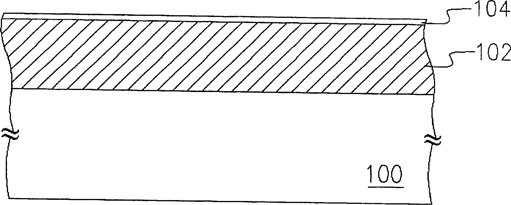
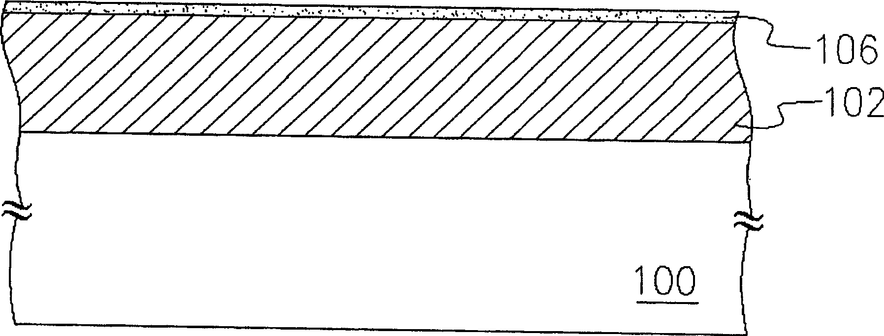
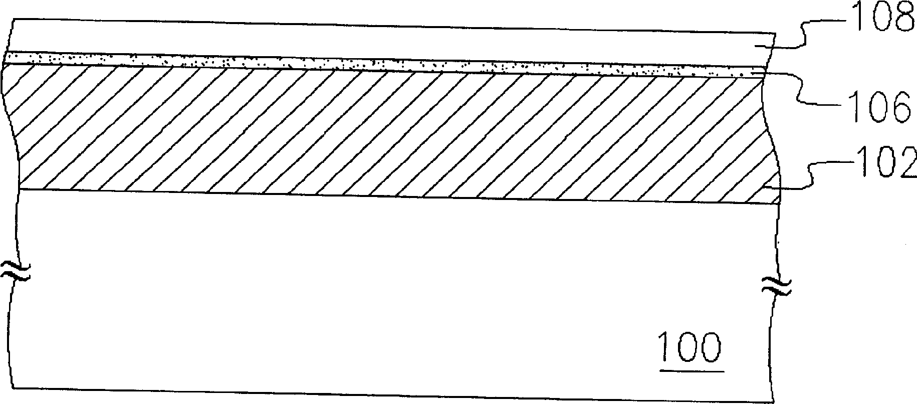
[0023] The present invention is a method for manufacturing a dielectric layer, which is described here by taking the manufacture of a capacitor as an example.

[0024] Figure 1A to Figure 1D It is a flowchart of a manufacturing method of a capacitor according to a preferred embodiment of the present invention.

[0025] Please refer to Figure 1A , a substrate 100 is provided, such as a silicon substrate, and a part of the semiconductor device has been fabricated on the substrate 100, such as a metal-oxide-semiconductor transistor (not shown) has been fabricated. Next, a lower electrode layer 102 of a capacitor is formed on the substrate 100 . The material of the bottom electrode layer 102 is, for example, polysilicon, and its formation method is, for example, chemical vapor deposition, or a part of the silicon substrate is monocrystalline silicon as the bottom electrode. After the lower electrode layer 102 is formed, the surface of the lower electrode layer 102 will undergo...


PUM


Abstract

The invention is a dielectric layer making method, placing a substrate in a furnace tube and developing a silicon oxide layer on the substrate, then converting the silicon oxide layer into a silicon oxynitride layer, then, developing a silicon oxide layer on the silicon oxynitride, and a silicon oxynitride/silicon nitride/silicon oxide overlapped layer dielectric layer on the substrate. The technique is completed in the same furnace tube.

Description

technical field [0001] The invention relates to a method for manufacturing a dielectric layer applied on a semiconductor element, and in particular to a method for manufacturing a capacitor dielectric layer. Background technique [0002] When the integration level of the entire semiconductor device is getting higher and higher, the area of ​​the storage unit of the Dynamic Random Access Memory (DRAM) is also getting smaller and smaller. Therefore, how to increase the charge storage capacity of the capacitor in the DRAM memory unit in a limited area has become an important issue. [0003] In general, methods to increase the charge storage capacity of capacitors include increasing the area of ​​the capacitor, reducing the thickness of the dielectric layer of the capacitor, and using dielectric materials with high dielectric constants. However, increasing the area of ​​the capacitor will reduce the integration of DRAM; reducing the thickness of the capacitor dielectric layer i...

Claims


Application Information

Patent Timeline
Patent Type & Authority Applications(China)
IPC IPC(8): H01L21/314
Inventor 巫勇贤李政哲
Owner PROMOS TECH INC
Why Eureka
Try Eureka