

Epitaxial structure with interposed layer quantum well semiconductor laser
A technology of epitaxial structure and insertion layer, applied in the field of epitaxial structure, can solve the problem of difficult to obtain interface quality quantum well and quantum barrier layer and so on
- Summary
- Abstract
- Description
- Claims
- Application Information
AI Technical Summary
Problems solved by technology
Method used
Image

Examples
Embodiment 1
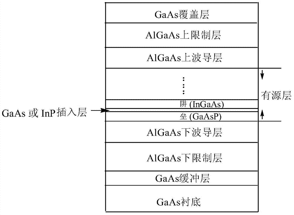
[0010] Reference attached figure 1 , The invention relates to an epitaxial structure of a semiconductor laser with an insertion layer quantum well, and the invention discloses a preparation method of a semiconductor laser with a special structure. The structure includes from bottom to top: GaAs substrate; GaAs buffer layer; AIGaAs lower confinement layer; AIGaAs lower waveguide layer; active layer is InGaAs / GaAsP (the insertion layer in the active layer is GaAs or InP); Waveguide layer; AIGaAs upper confinement layer; GaAs cladding layer. In this structure, a thin layer of GaAs or InP is inserted between the quantum well of the active layer and the barrier, which can effectively alleviate the lattice adaptation between the quantum well and the barrier, improve the interface quality, reduce the stress, and obtain a higher The low threshold current density improves the optoelectronic performance of semiconductor laser devices.
Embodiment 2
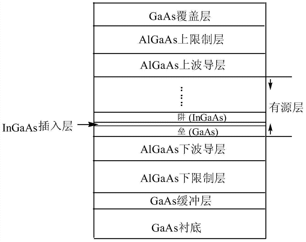
[0012] Reference attached figure 2 , The invention relates to an epitaxial structure of a semiconductor laser with an insertion layer quantum well, and the invention discloses a preparation method of a semiconductor laser with a special structure. The structure includes from bottom to top: GaAs substrate; GaAs buffer layer; AIGaAs lower confinement layer; AIGaAs lower waveguide layer; layer); AIGaAs upper waveguide layer; AIGaAs upper confinement layer; GaAs cladding layer. The content of In in the InGaAs insertion layer with relatively low content of In is between 0.02 and 0.1 (mole mass fraction). The period number of the active layer is 5-10, and the In content is between 0.16-0.2 (mole mass fraction). In this structure, a thin layer of InGaAs is inserted between the quantum wells and the barriers of the active layer, which can effectively reduce the lattice mismatch between the quantum wells and the barriers, smooth the interface components, and eliminate stress, thereb...
PUM
 Abstract
Description
Claims
Application Information