Semiconductor structure, forming method thereof and field effect transistor

A technology of semiconductors and nitride semiconductors, which is applied in the direction of semiconductor devices, semiconductor/solid-state device manufacturing, electrical components, etc., can solve the problems that the structure design and preparation methods need to be improved, so as to improve the interface defects, simplify the preparation process and equipment requirements, reduce the cost effect

Inactive Publication Date: 2016-04-20
TSINGHUA UNIV
View PDF3 Cites 8 Cited by
  • Summary
  • Abstract
  • Description
  • Claims
  • Application Information

AI Technical Summary

Problems solved by technology

[0005] However, the current structural design and preparation methods of semiconductor structures based on gallium nitride material series still need to be improved.

Method used


Image

  • Semiconductor structure, forming method thereof and field effect transistor
  • Semiconductor structure, forming method thereof and field effect transistor
  • Semiconductor structure, forming method thereof and field effect transistor

Examples


Embodiment 1

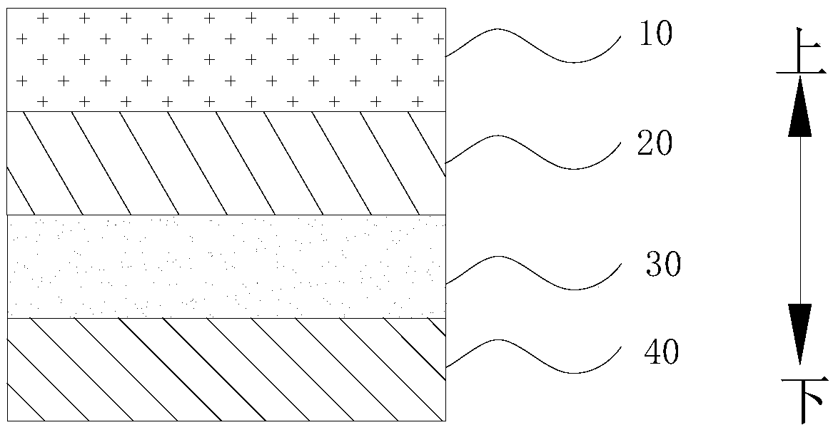
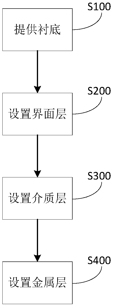
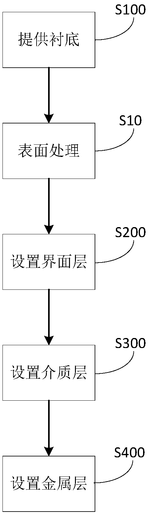
[0070] Embodiment 1 Preparation of GaN substrate semiconductor structure

[0071] A GaN free-standing wafer was chosen as the substrate. In addition, one surface of the GaN self-supporting wafer is a nonpolar m-plane. Concrete preparation process is as follows:

[0072] i. Soak the GaN substrate sample sequentially in acetone and alcohol heated in a water bath at 65 degrees Celsius for 20 minutes.

[0073] ii. Rinse with deionized water for 10 minutes, soak in isopropanol for five minutes.

[0074] iii. Prepare the aqua regia solution, put the aqua regia solution into a water bath at 65 degrees Celsius, and put the GaN sample in the aqua regia for 40 minutes to remove the natural oxide on the surface.

[0075] iii. Rinse the substrate with deionized water for 10 minutes, soak in isopropanol for 5 minutes, and blow dry with nitrogen.

[0076] v. Immediately place the cleaned sample into the ALD chamber for deposition. Aluminum nitride is deposited on the m-plane GaN, and N...

Embodiment 2

[0078] Embodiment 2 Preparation of GaN substrate semiconductor structure

[0079] A gallium nitride free-standing wafer was chosen as the substrate. In addition, one side surface of the gallium nitride self-supporting wafer is a nonpolar a-plane. All the other preparation processes are the same as in Example 1.


PUM

PropertyMeasurementUnit
thicknessaaaaaaaaaa
thicknessaaaaaaaaaa
thicknessaaaaaaaaaa

Abstract

The invention discloses a semiconductor structure, a forming method thereof and a field effect transistor. The semiconductor structure comprises a substrate, an interface layer, a dielectric layer and a metallic layer, wherein at least a part of the upper surface of the substrate is a nonpolar face or semipolar face formed by a nitride semiconductor crystal; the interface layer is formed on the nonpolar face or semipolar face and is prepared from either a nitride or a nitric oxide; the dielectric layer is formed on the surface, far away from the substrate, of the interface layer; the metallic layer is formed on the surface, far away from the interface layer, of the dielectric layer. Thus, the interface layer can be formed on the nonpolar face or semipolar face of the surface of the substrate, then, unstable chemical bonds can be effectively prevented from being formed on the surface of the substrate, the interface quality is improved, and then, the interface performance of the semiconductor structure can be effectively improved.

Description

technical field [0001] The invention relates to the field of semiconductor technology and semiconductor manufacturing, in particular, the invention relates to a semiconductor structure, a method for forming the semiconductor structure and a field effect transistor. Background technique [0002] Nitride semiconductor series materials represented by gallium nitride (GaN) (GaN, InGaN, AlGaN, InN, and AlN, etc.) have wide direct band gaps, strong atomic bonds, high thermal conductivity, and good chemical stability ( Almost not corroded by any acid) and strong radiation resistance, it has broad prospects in the application of optoelectronics, high-temperature high-power devices and high-frequency microwave devices, and is widely used in the preparation of various electronic switches and various signal amplifier. [0003] Generally, nitride semiconductor materials have a close-packed hexagonal crystal structure. According to the relative positional relationship between the wafer ...

Claims


Application Information

Patent Timeline
Patent Type & Authority Applications(China)
IPC IPC(8): H01L29/78H01L21/336H01L29/04H01L29/20
CPCH01L29/78H01L29/045H01L29/2003H01L29/66446H01L29/66477
Inventor 武娴郭磊王敬
Owner TSINGHUA UNIV
Why Eureka
Try Eureka