Optical transceiver having enhanced EMI tolerance

a technology of optical transceivers and emi radiation, which is applied in the direction of electromagnetic transceivers, optical elements, instruments, etc., can solve the problems of leakage of emi radiation with higher frequencies, no room to place such a shielding member, and leakage of emi radiation

Active Publication Date: 2013-05-30
SUMITOMO ELECTRIC IND LTD
View PDF1 Cites 10 Cited by
  • Summary
  • Abstract
  • Description
  • Claims
  • Application Information

AI Technical Summary

Problems solved by technology

However, recent optical transceiver operates in a higher frequency, sometimes exceeding 10 GHz; a small gap causes the leak of the EMI radiation from the optical transceiver.
For instance, misalignment between the face panel and the cage may leak the EMI radiation.
Moreover, the conventional ground fingers inherently have a gap with respect to adjacent fingers, which may also cause the leak of the EMI radiation with higher frequencies.
Although some optical connectors implement a member to shield such a gap, a small sized connector applied in recent systems often have no room to place such a shielding member.
Thus, a way to implement an auxiliary member to shield a small gap shows a limitation as the operating frequency becomes higher.

Method used


Image

  • Optical transceiver having enhanced EMI tolerance
  • Optical transceiver having enhanced EMI tolerance
  • Optical transceiver having enhanced EMI tolerance

Examples


first embodiment

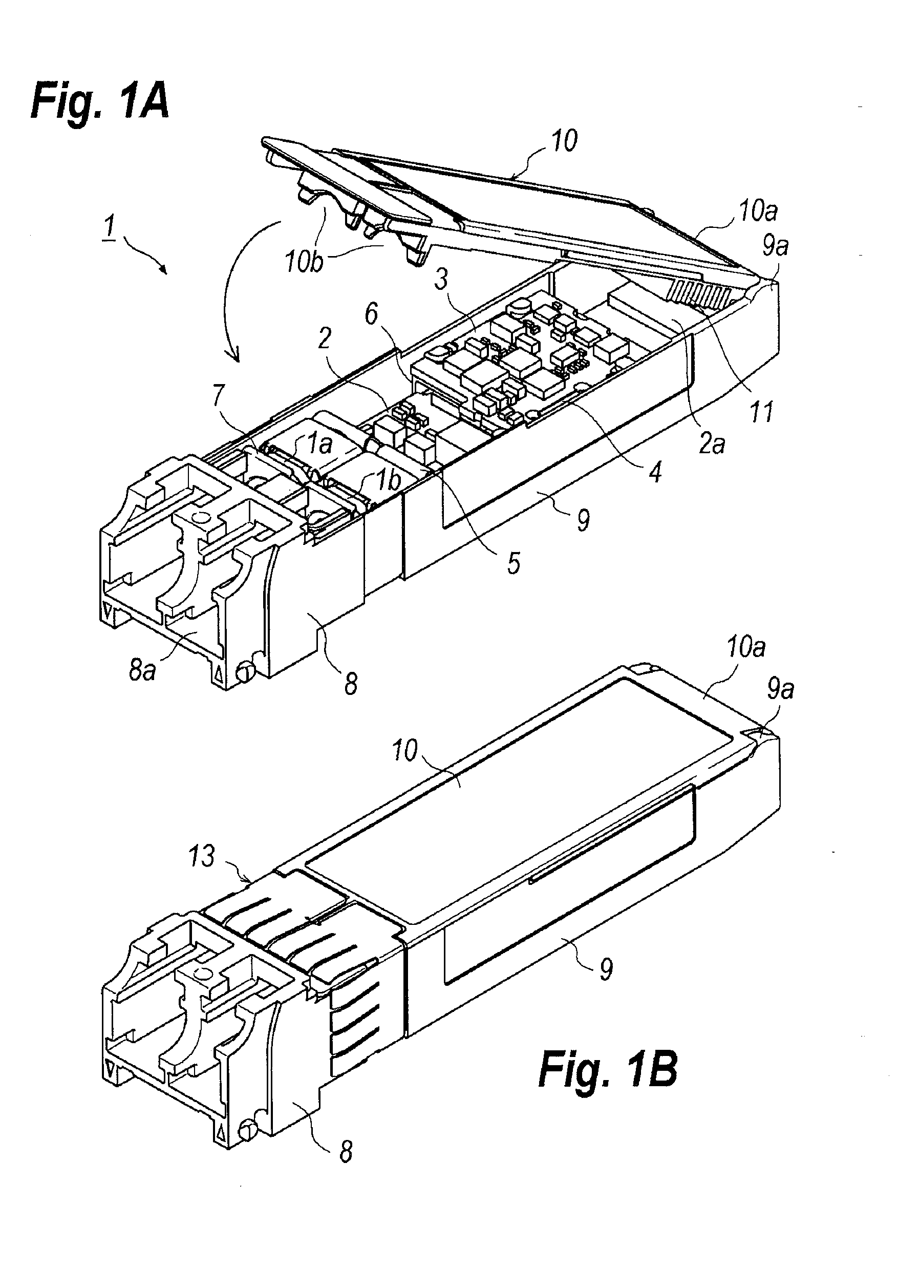
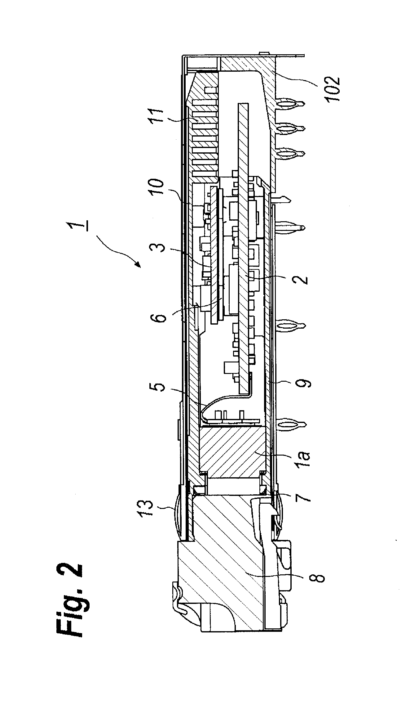
[0033]FIGS. 1A and 1B are perspective views of an optical transceiver 1 of the present invention, where FIG. 1A opens the top cover 10 thereof, while, FIG. 1B closes the top cover 10 and attaches the ground finger 13 in a front portion of the top cover 10. FIG. 2 is a cross section taken along the longitudinal axis of the optical transceiver 1, in which the optical transceiver 1 is set within a cage 102 prepared in the host system.

[0034]The optical transceiver 1 includes a TOSA 1a, a ROSA 1b, a motherboard 2, a daughter board 3, flexible printed circuit (hereafter denoted as FTC) boards 5, a shield member 7, an optical receptacle 8, a bottom base 9, the top cover 10, a combed structure 11, and the ground finger 13. The description below assumes that the “front” corresponds to a side where the optical receptacle 8 is provided, while, the “rear” is an opposite side where the combed structure and an electrical plug 2a is provided.

[0035]The TOSA 1a and the ROSA 1b are arranged in side-b...

second embodiment

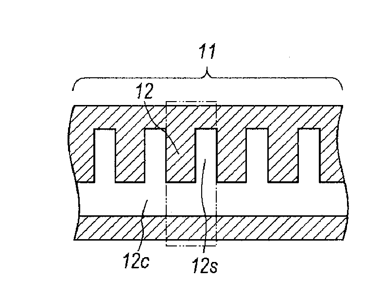
[0054]FIG. 11A is a perspective view showing still another embodiment of the according to the present invention. A feature of the present embodiment is that the bottom base 9D provides in a rear portion of the bottom plate 9c thereof close to the electrical plug a modified combed structure 11D including a plurality of fins, while, the top cover 10D also provides in the rear portion of the top plate 10c thereof corresponding to the rear portion of the bottom base 9D the combed structure 11D with a plurality of fins 12d. These combed structure 11D is covered by rear cover 9e assembled with the bottom base 9D in the side 9d thereof. The bottom base 9D, the top cover 10D, and the rear cover 9e are also made of metal to realize the functions of the heat conduction and the EMI shield.

[0055]Each of the fins 12d has a cross section of the T-shape viewed from the side of the optical transceiver. The combed structure 11D shown in FIGS. 11A and 11B has the function to attenuate the EMI radiati...


PUM


Abstract

An optical transceiver that attenuates the EMI radiation leaked therefrom is disclosed. The optical transceiver includes a top cover and the bottom base to form a cavity into which a TOSA, a ROSA, and a circuit are set. At least one of the top cover and the bottom base provides a combed structure in a rear portion of the optical transceiver, where the combed structure has a plurality of T-shaped fins to attenuate the EMI radiation.

Description

CROSS REFERENCE TO RELATED APPLICATIONS[0001]This patent application is a continuation-in-part of pending prior U.S. patent application Ser. No. 13 / 578,841, filed Aug. 14, 2012 by Oomori et al. for OPTICAL TRANSCEIVER HAVING ENHANCED EMI TOLERANCE, which is a National Stage application of PCT / JP2011 / 079975, filed Dec. 16, 2011, which claims priority to Japanese Patent Application No 2010-282719, filed Dec. 20, 2010, all of which are hereby incorporated herein by reference in their entirety. This patent application also claims priority to Japanese Patent Application No. 2012-011624, filed Jan. 24, 2012, which is also hereby incorporated by reference in its entirety.BACKGROUND OF THE INVENTION[0002]1. Field of the Invention[0003]The present invention relates to an optical transceiver, in particular, the invention relates to an optical transceiver with an enhanced electro-magnetic interference (hereafter denoted as EMI) tolerance.[0004]2. Background Art[0005]An optical transceiver gene...

Claims


Application Information

Patent Timeline
Patent Type & Authority Applications(United States)
IPC IPC(8): H04B10/40
CPCH04B10/40H05K9/0058G02B6/4227
Inventor KAWASE, DAISUKEISHII, KUNIYUKIOOMORI, HIROYASUKURASHIMA, HIROMI
Owner SUMITOMO ELECTRIC IND LTD
Why Eureka
Try Eureka