Nonvolatile memory device
- Summary
- Abstract
- Description
- Claims
- Application Information
AI Technical Summary
Benefits of technology
Problems solved by technology
Method used
Image
Examples
first embodiment
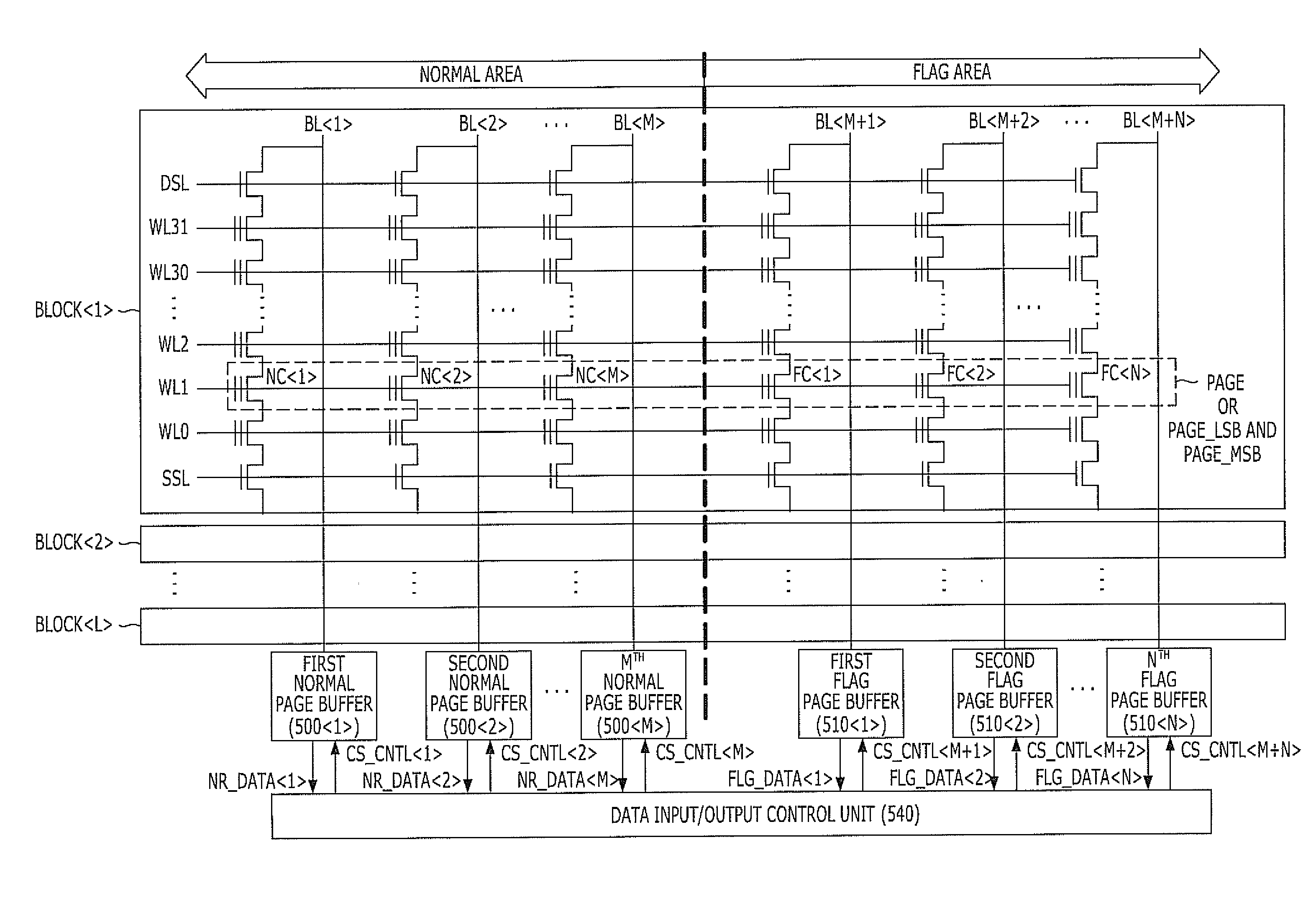
[0032]FIG. 5 is a block diagram illustrating the configuration of a nonvolatile memory device in accordance with a first embodiment of the present invention.
[0033]Referring to FIG. 5, a nonvolatile memory device in accordance with a first embodiment of the present invention includes a page PAGE, M number of normal page buffers 500, N number of flag page buffers 510, and a data input / output control unit 540.
[0034]For reference, a plurality of blocks BLOCK are included in a memory cell array of the nonvolatile memory device. A plurality of word lines WL and a plurality of bit lines BL and BL are arranged in an array type in each of the plurality of blocks BLOCK, and nonvolatile memory cell transistors are disposed at respective crossing points. When each of a plurality of memory cell transistors NC and FC connected to each word line of the plurality of word lines WL can store 1-bit data, and data reading and writing are simultaneously performed for, the plurality of memory cells NC an...
second embodiment
[0062]FIG. 6 is a block diagram illustrating the configuration of a nonvolatile memory device in accordance with a second embodiment of the present invention.
[0063]Referring to FIG. 6, a nonvolatile memory device in accordance with a second embodiment of the present invention includes a word line WL1>, M number of normal page buffers 600, N number of flag page buffers 610, and a data input / output control unit 640. The word line WL1> includes K number of pages PAGE.
[0064]For reference, a plurality of blocks BLOCK are included in a memory cell array of the nonvolatile memory device. A plurality of word lines WL and a plurality of bit lines BL_EVEN, BL_ODD, BL_EVEN and BL_ODD are arranged in an array type in each of the plurality of blocks BLOCK, and nonvolatile memory cell transistors are disposed at respective crossing points. When each of a plurality of memory cell transistors NCE, NCO, FCE, and FCO connected to each word line of the plurality of word lines WL can store 1-bit data, ...
third embodiment
[0102]FIG. 7 is a block diagram illustrating the configuration of a nonvolatile memory device in accordance with a third embodiment of the present invention.
[0103]Referring to FIG. 7, a nonvolatile memory device in accordance with a third embodiment of the present invention includes a first word line WL1>, a second word line WL2>, M number of normal page buffers 700, N number of flag page buffers 710, and a data input / output control unit 640. The word line WL1>includes K number of pages PAGE.
[0104]For reference, a plurality of blocks BLOCK are included in a memory cell array of the nonvolatile memory device. A plurality of word lines WL and a plurality of bit lines BL_EVEN, BL_ODD, BL_EVEN, BL_ODD are arranged in an array type in each of the plurality of blocks BLOCK, and nonvolatile memory cell transistors are disposed at respective crossing points. When each of a plurality of memory cell transistors NCE, NCO, FCE, and FCO connected to each word line of the plurality of word lines ...
PUM
 Abstract
Description
Claims
Application Information


