

Mold for nanoimprint lithography
- Summary
- Abstract
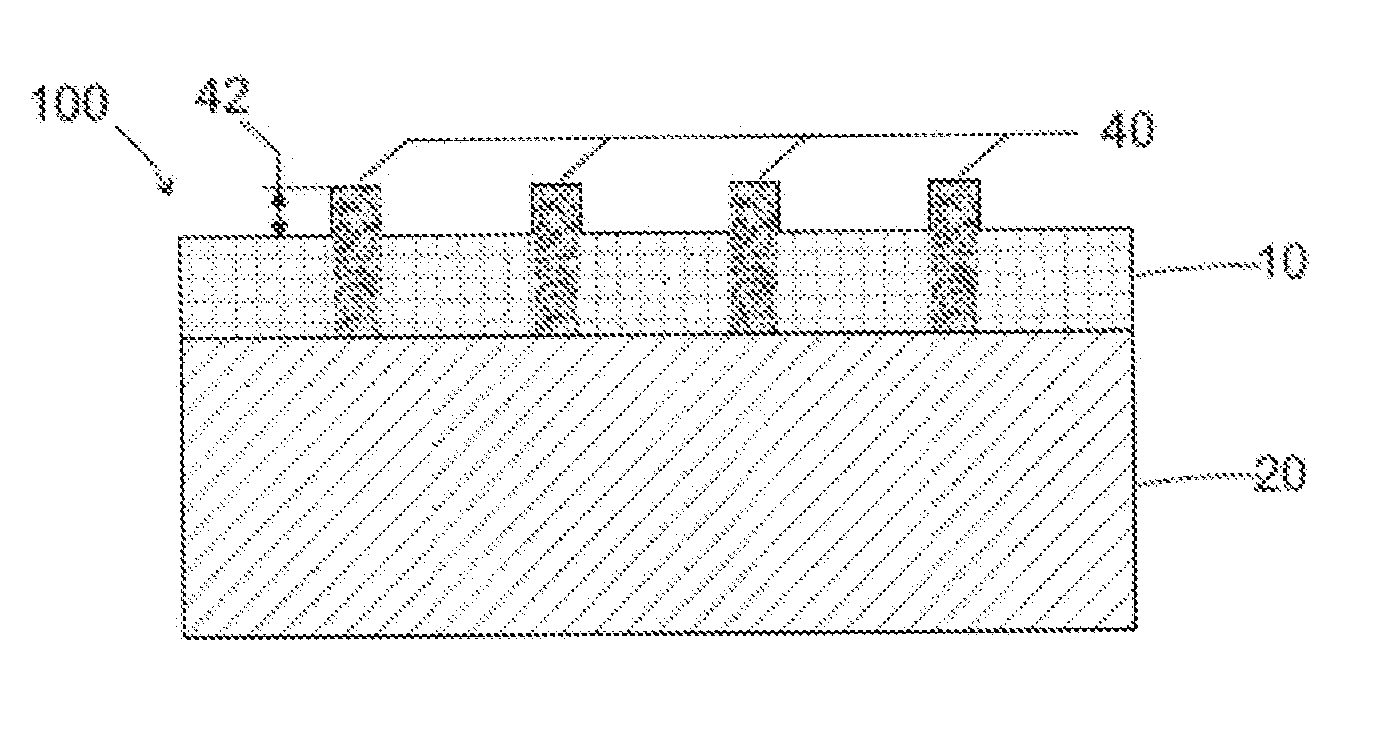
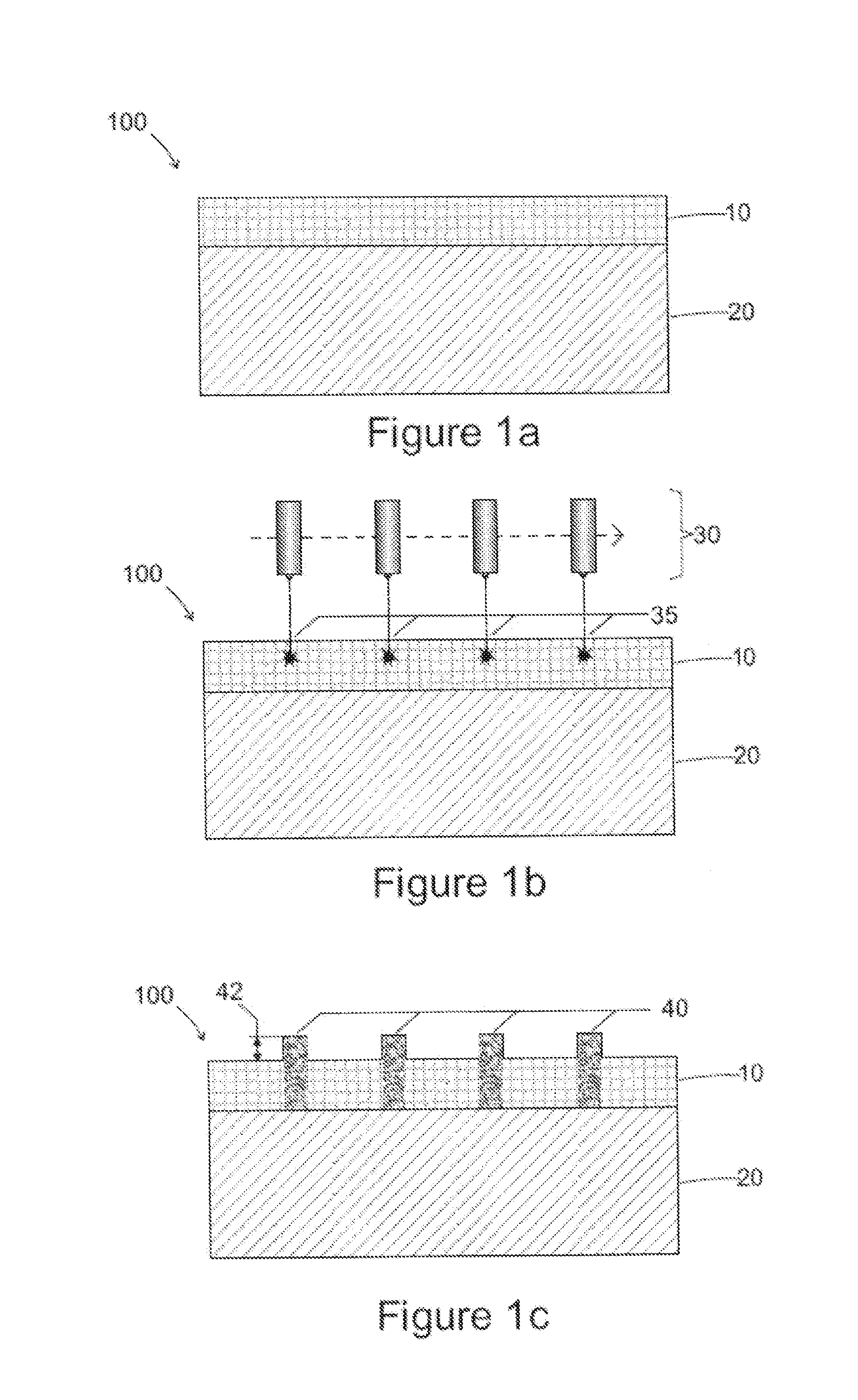
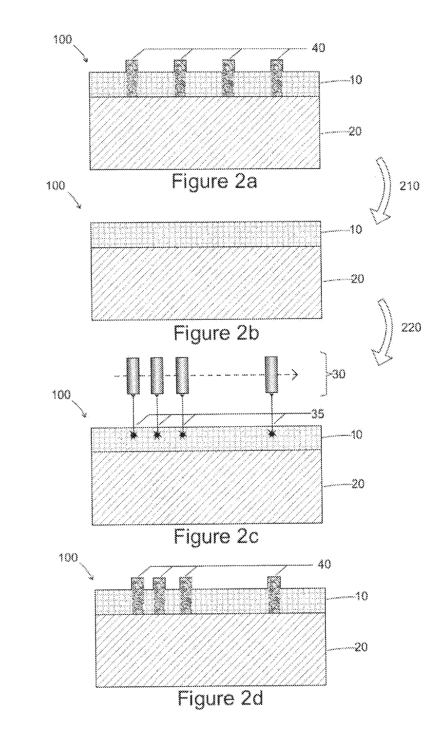
- Description
- Claims
- Application Information
AI Technical Summary
Benefits of technology
Problems solved by technology
Method used
Image

Examples
Embodiment Construction
[0033]Before a detailed review of embodiments of the invention is begun, the optional characteristics that may be used in association or alternatively will be listed hereinafter:
[0034]Preferably the layer of phase-changing material is at least partly in its crystalline phase before the personalization step.
[0035]Advantageously the formation of patterns is achieved by local irradiation of the layer of phase-changing material by means of a writing laser.
[0036]Preferably the layer of phase-changing material exhibits a volume increase greater than 4% and preferably greater than 5% between its crystalline phase and its amorphous phase.
[0037]According to one embodiment, the step of at least partial erasure is applied to all the patterns. Preferably the erasure step is performed in an annealing furnace, which completely restores the layer of phase-changing material to its crystalline phase, thus causing all patterns to disappear.
[0038]According to another embodiment, the erasure step is lo...
PUM
| Property | Measurement | Unit |
|---|---|---|
| Fraction | aaaaa | aaaaa |
| Fraction | aaaaa | aaaaa |
| Transparency | aaaaa | aaaaa |
Abstract
Description
Claims
Application Information