Electronic textile and method of manufacturing an electronic textile

a technology of electronic textiles and textile substrates, applied in the field of electronic textiles, can solve the problems of difficult to mount electronic components on textile substrates in a reliable and cost-efficient manner, unsuitable for mass production, and affecting the quality of textiles, and achieve the effect of cost-efficient production

Inactive Publication Date: 2013-07-11
SIGNIFY HLDG BV +1
View PDF7 Cites 30 Cited by
  • Summary
  • Abstract
  • Description
  • Claims
  • Application Information

AI Technical Summary

Benefits of technology

[0007]In view of the above-mentioned and other drawbacks of the prior art, a general object of the present invention is to enable a more cost-efficient production of electronic textiles.

Problems solved by technology
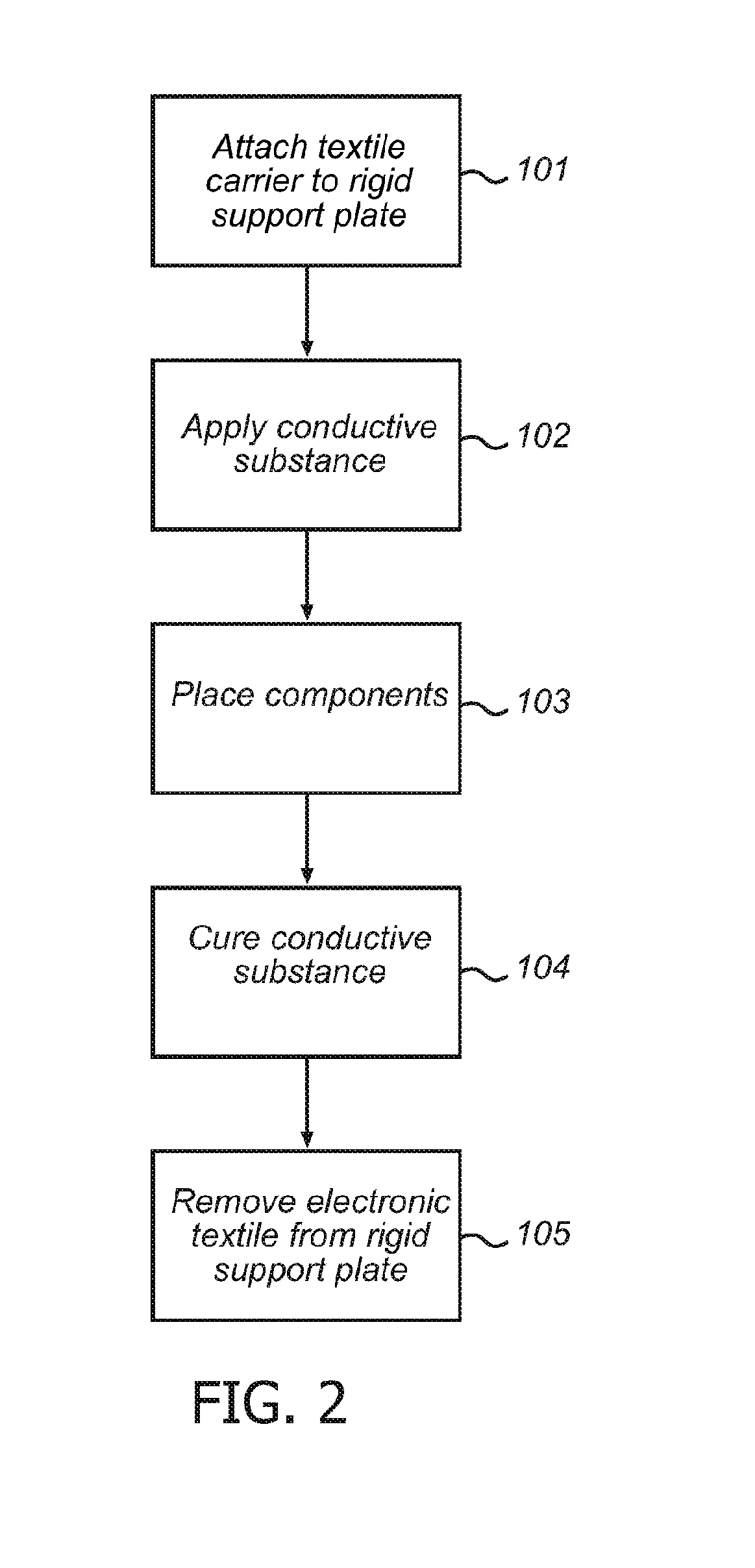
However, the very same properties as well as irregularities in the textile resulting from the manufacturing process translate to challenges faced in the process of devising a process for manufacturing an electronic textile.
For example, it has turned out to be difficult to mount electronic components on a textile substrate in a reliable and cost-efficient manner.
However, most of these methods are labor intensive and are not suitable for mass-production, at least not without extensive investment in new types of manufacturing equipment.
Although appearing to be able to handle a high production rate, the method disclosed by WO-2010 / 033902 seems to require a special type of electronic component package and utilizes a connection technique which is not a standard in the electronics manufacturing industry.
Accordingly, substantial investment would be required to use the method of WO-2010 / 033902 and it would be possible to use only custom made component packages, which increases the cost of the electronic textile.

Method used


Image

  • Electronic textile and method of manufacturing an electronic textile
  • Electronic textile and method of manufacturing an electronic textile
  • Electronic textile and method of manufacturing an electronic textile

Examples


Embodiment Construction

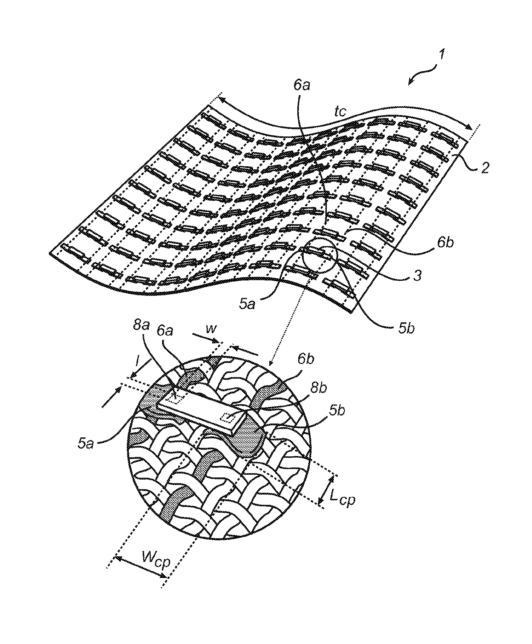
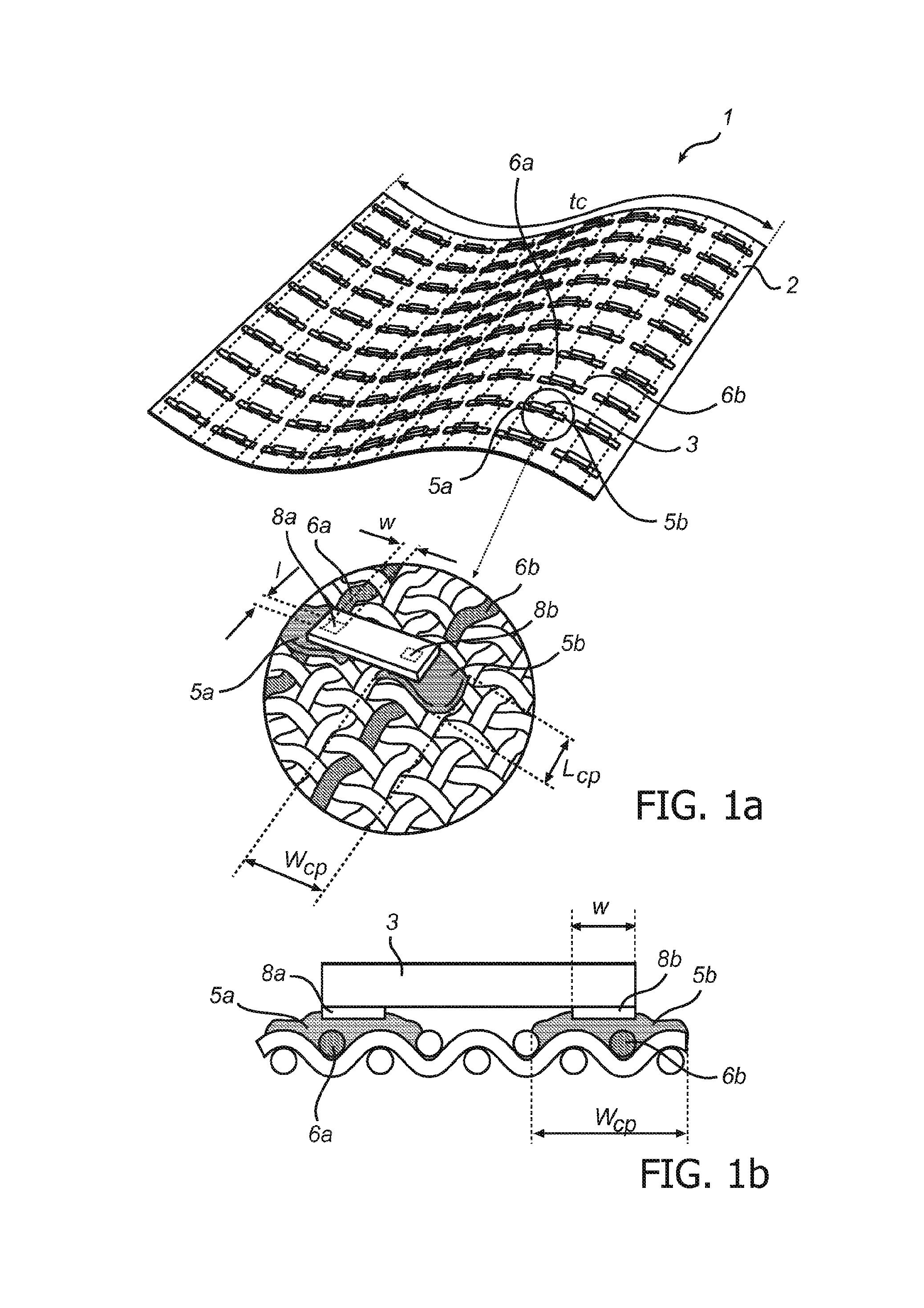
[0030]FIG. 1a schematically illustrates an exemplary electronic textile 1 comprising a textile carrier 2 and a plurality of electronic components, here in the form of light-emitting diodes (LEDs) 3 (only one of these is indicated in the drawing to avoid cluttering the drawing). In the exemplary embodiment shown in FIGS. 1a-b, the textile carrier 2 is provided in the form of a woven fabric comprising interwoven conductive yarns and non-conductive yarns.

[0031]On the textile carrier 2, a plurality of sets of connection pads 5a-b are provided such that a first connection pad 5a overlaps a first conductor line 6a, and the second connection pad 5b overlaps a second conductor line 6b, which is substantially parallel with the first conductor line 6a (again, only one set of connection pads and associated conductor lines are indicated in the drawing to avoid cluttering the drawing). Each LED 3 is electrically connected to a pair of conductor lines 6a-b. The conductor lines may be interrupted ...


PUM

PropertyMeasurementUnit
lengthaaaaaaaaaa
widthaaaaaaaaaa
conductiveaaaaaaaaaa

Abstract

A method of manufacturing an electronic textile (1) comprising the steps of: providing a textile carrier (2) comprising a plurality of conductor lines (6a-b); releasably attaching (101) the textile carrier (2) to a rigid support plate (20); providing (102) a conductive substance on the textile carrier (2) in a pattern forming a plurality of sets of connection pads (5a-b) on the textile carrier (2), each set of connection pads defining a component placement position for placement of an electronic component (3), and each set of connection pads (5a-b) comprising a connection pad overlapping one of the conductor lines, the connection pad having a connection pad length (Lcp) in a direction parallel to the conductor line and a connection pad width (Wcp) in a direction perpendicular to the conductor line, wherein the connection pad width (Wcp) is at least one percent of an extension (Wtc) of the textile carrier (2) in the direction perpendicular to the conductor line; automatically placing (103) electronic components (3) at the component placement positions; curing (104) the conductive substance to attach the electronic components (3) to the textile carrier (2), thereby forming the electronic textile (1) and removing (105) the electronic textile from the rigid support plate.

Description

FIELD OF THE INVENTION[0001]The present invention relates to an electronic textile, and to a method of manufacturing such an electronic textile.BACKGROUND OF THE INVENTION[0002]Many types of textiles are used in our every-day life. When electronics are unobtrusively integrated into these textiles to create electronic textiles, new application fields emerge. One such example of a new application is light-emitting textiles, and other examples include textile-based sensing systems, wearable electronics etc.[0003]For these new applications, the very special properties of a textile, such as the conformability and / or stretchability that can be achieved with a textile are advantageous. However, the very same properties as well as irregularities in the textile resulting from the manufacturing process translate to challenges faced in the process of devising a process for manufacturing an electronic textile. For example, it has turned out to be difficult to mount electronic components on a te...

Claims


Application Information

Patent Timeline
Patent Type & Authority Applications(United States)
IPC IPC(8): H05K1/02F21V21/00H05K3/30
CPCH05K1/038H05K1/189H05K2201/0281H05K2201/029H05K2201/10106Y10T29/4913F21V21/00H05K1/0277H05K3/303H05K1/0283H05K3/321H05K2203/0152F21K9/20H05K1/111H05K1/181
Inventor ZHOU, GUOFURADEMAKERS, JOHANNES ANDRIANUS MARIASNOEIJEN, PETRUS ANTONIUS HENRICUSBAX, JOSEPHUS HENRICUS GERARDUSVAN ABEELEN, FRANK ANTONVAN PIETERSON, LIESBETH
Owner SIGNIFY HLDG BV
Why Eureka
Try Eureka