Touch panel comprising an electrically-conductive pattern and a production method therefor

Active Publication Date: 2013-08-22
LG CHEM LTD
View PDF10 Cites 49 Cited by
  • Summary
  • Abstract
  • Description
  • Claims
  • Application Information

AI Technical Summary

Benefits of technology

[0010]According to exemplary embodiments of the present invention, in a touch panel comprising a conducting pattern provided in an effective picture portion, it is possible to prevent reflection by the conducting pattern without affecting conductivity of the conducting pattern by introducing a light abso

Problems solved by technology

In general, an electrostatic capacitance type touch panel uses an ITO-based conducting film, but the ITO has disadvantages in that, a realization speed is low by a RC delay of the ITO when applying the ITO to a large area touch panel, such that it is difficult to apply the ITO to the large area.
In addition, in the case where a touch screen is manufactured by using a film on which the ITO is deposited, it is not easy to treat the touch screen due to cracks by bending of the ITO film.
Among the disadvantages, i

Method used


Image

  • Touch panel comprising an electrically-conductive pattern and a production method therefor
  • Touch panel comprising an electrically-conductive pattern and a production method therefor
  • Touch panel comprising an electrically-conductive pattern and a production method therefor

Examples


Example

Experimental Example 1

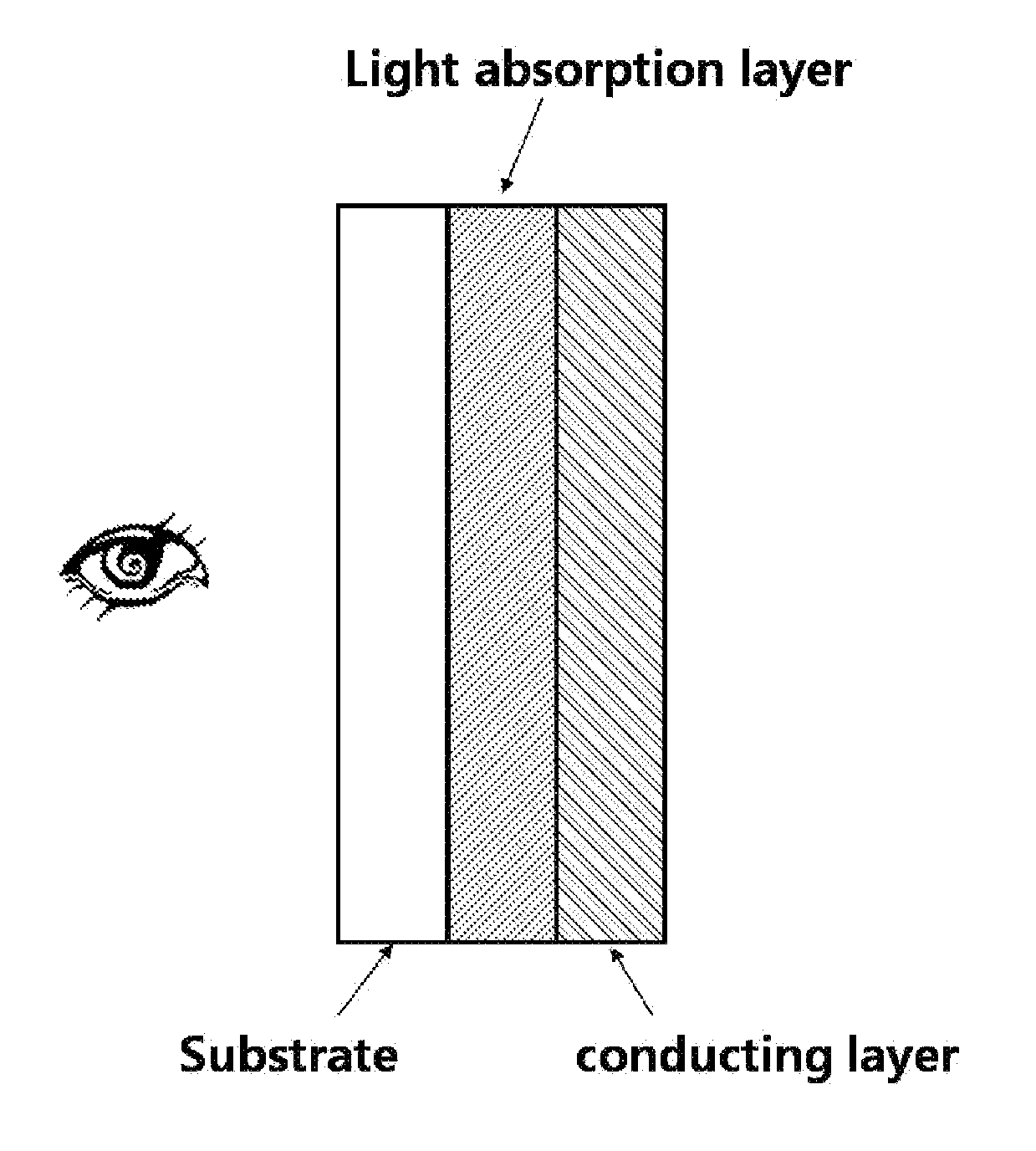
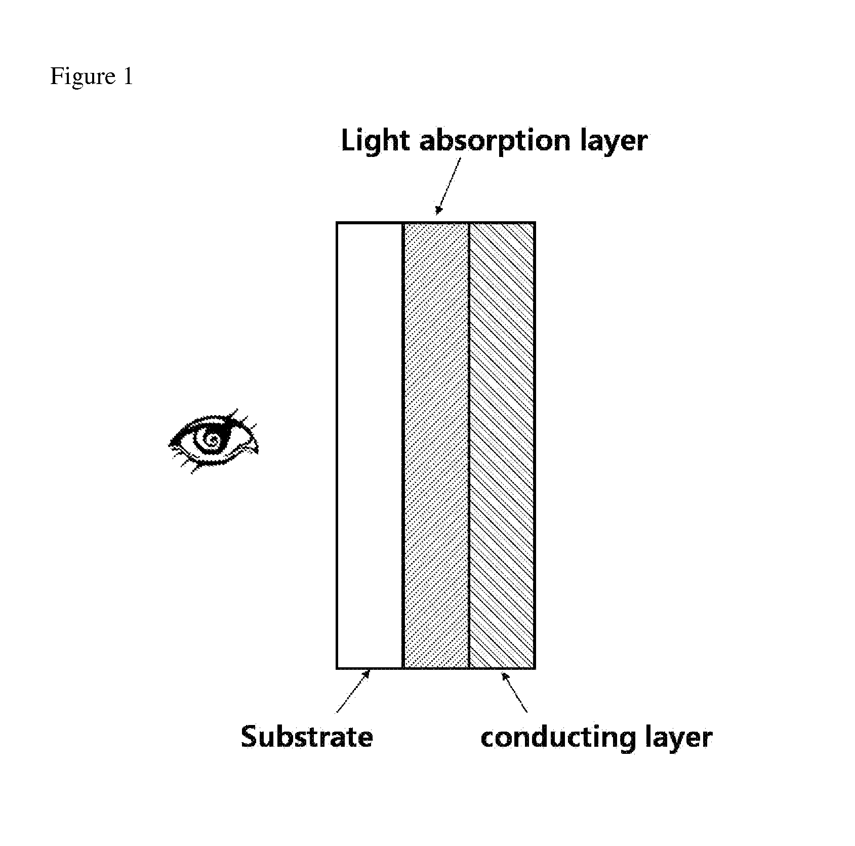
[0115]After the light absorption layer formed by using the Mo-based oxynitride was formed on the substrate, the conducting layer was formed thereon by using Cu. Subsequently, in order to measure the total reflectance, the entire surface black treatment was performed on the upper surface of the conducting layer, and the total reflectance (specular reflection / 550 nm) was measured by irradiating visible rays from the substrate. In this case, the reflectance was 6.1%. The laminate according to Experimental Example 1 was illustrated in FIG. 8.

Example

Experimental Example 2

[0116]After the light absorption layer formed by using the Al-based oxynitride was formed on the substrate, the conducting layer was formed thereon by using Al. Subsequently, in order to measure the total reflectance, the entire surface black treatment was performed on the upper surface of the conducting layer, and the total reflectance (specular reflection / 550 nm) was measured by irradiating visible rays from the substrate. In this case, the reflectance was 2.1%.

Example

Experimental Example 3

[0117]After the light absorption layer formed by using the Cu-based oxynitride was formed on the substrate, the conducting layer was formed thereon by using Cu. Subsequently, in order to measure the total reflectance, the entire surface black treatment was performed on the upper surface of the conducting layer, and the total reflectance (specular reflection / 550 nm) was measured by irradiating visible rays from the substrate. In this case, the reflectance was 6%.


PUM


Abstract

The present invention relates to a touch panel comprising a structure body comprising: a substrate; a conducting pattern that is provided on at least one surface of the substrate; and a light absorption pattern provided on at least one surface of the conducting pattern and provided on at least a portion of regions corresponding to the conducting pattern, and a method for manufacturing the same.

Description

TECHNICAL FIELD[0001]This application claims priority from Korean Patent Application No. 10-2010-0102109 filed on Oct. 19, 2010 in the KIPO, the disclosure of which is incorporated herein by reference in its entirety.[0002]The present invention relates to a touch panel and a method for manufacturing the same. In detail, the present invention relates to a touch panel comprising a conducting pattern and a method for manufacturing the same. In more detail, the present invention relates to a touch panel in which a concealment property of a conducting pattern in constituting the touch panel by using the conducting pattern is improved, and a method for manufacturing the same.BACKGROUND ART[0003]In general, an electrostatic capacitance type touch panel uses an ITO-based conducting film, but the ITO has disadvantages in that, a realization speed is low by a RC delay of the ITO when applying the ITO to a large area touch panel, such that it is difficult to apply the ITO to the large area. In...

Claims


Application Information

Patent Timeline
IPC IPC(8): G06F3/041G02B5/00
CPCG02B5/003G06F3/044G06F3/0412G06F3/0443G06F2203/04103G06F3/0445G02B27/0018G02B27/021G02B27/022
Inventor HWANG, JI YOUNGHWANG, IN-SEOKCHUN, SANG KILEE, SEUNG HEON
Owner LG CHEM LTD
Why Eureka
Try Eureka