

Multilayer wiring board
a multi-layer wiring and mounting board technology, applied in the direction of printed circuit non-printed electric components, semiconductor/solid-state device details, high-frequency circuit adaptations, etc., can solve the problems of achieving the increase in signal line density and the propagation of high-frequency signals in the same board, and achieve the suppression of propagation signal degradation, high mounting density, and increased signal line density
Inactive Publication Date: 2013-09-12
TOHOKU UNIV +1
View PDF4 Cites 16 Cited by
- Summary
- Abstract
- Description
- Claims
- Application Information
AI Technical Summary
Benefits of technology
[0020]According to this invention, while maintaining high mounting density by a first wiring region, it is possible to suppress propagation signal degradation by a second wiring region when a high-frequency signal propagates for a long length. Therefore,
Problems solved by technology
However, since the propagation loss increases due to the increase in signal frequency and signal line density, it is difficult to ensure the reliability of a propagat
Method used
View moreImage
Smart ImageViewing Examples

Examples
 PUM
 Abstract
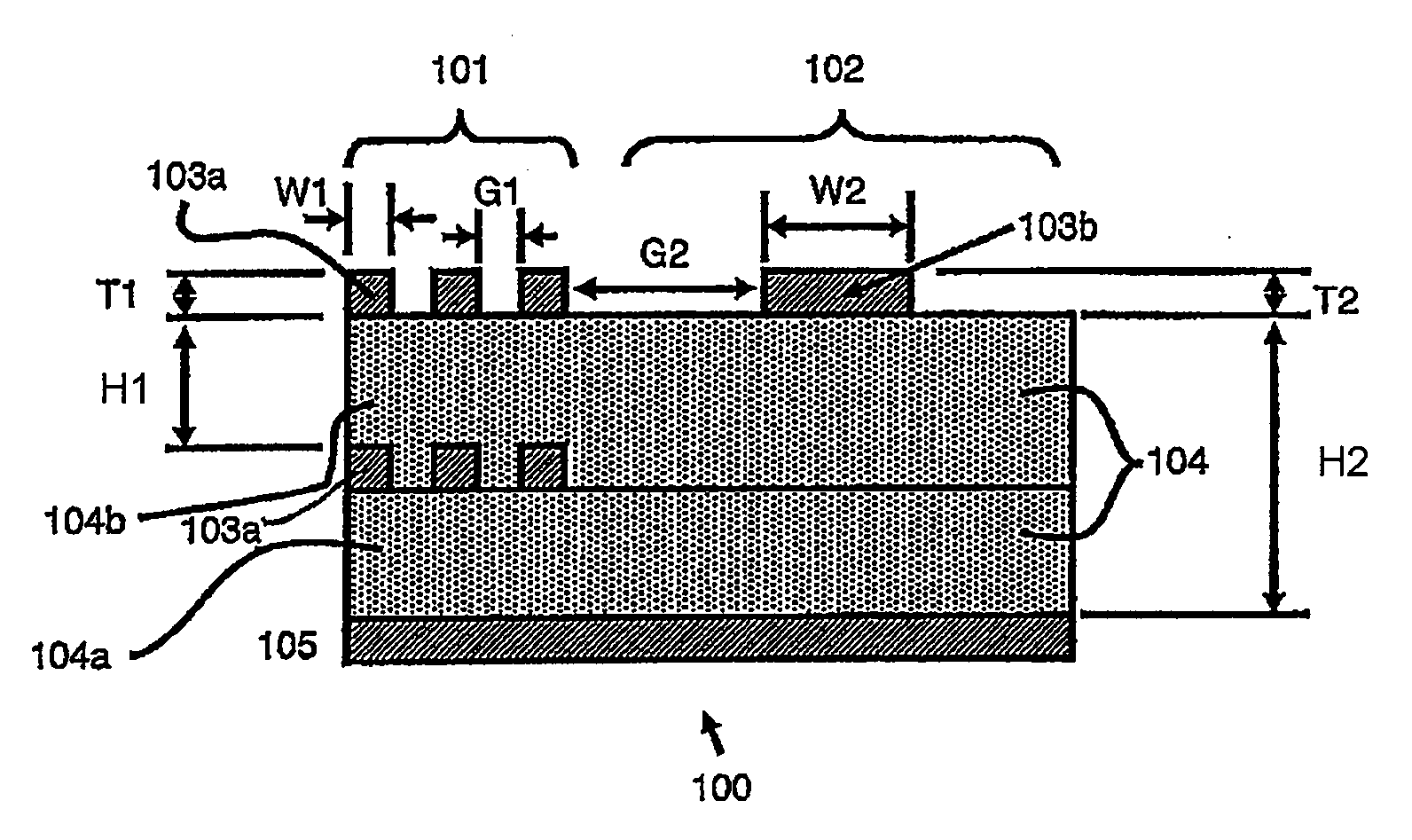
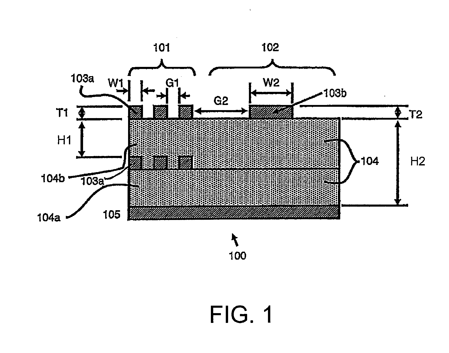
In a multilayer wiring board 100 having a high-density wiring region and a high-frequency propagation region mounted in the same board, it is possible to propagate a signal frequency of 40 GHz or more in the high-frequency propagation region by using a resin material with a dissipation factor (tan δ) of less than 0.01 as a material of an insulating layer used at least in the high-frequency propagation region. The insulating layer is formed of a polymerizable composition which contains a cycloolefin monomer, a polymerization catalyst, a cross-linking agent, a bifunctional compound having two vinylidene groups, and a trifunctional compound having three vinylidene groups and in which the content ratio of the bifunctional compound and the trifunctional compound is 0.5 to 1.5 in terms of a weight ratio value (bifunctional compound/trifunctional compound).
Description
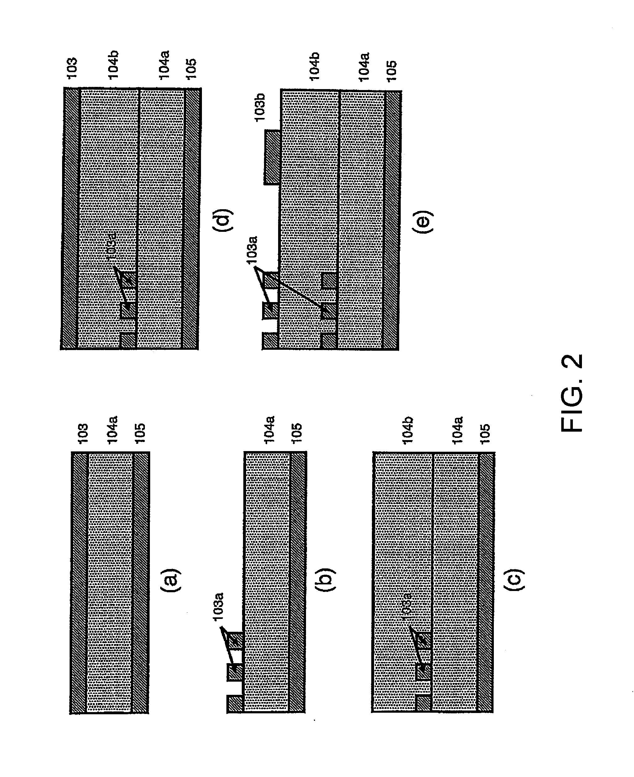
TECHNICAL FIELD[0001]This invention relates to a multilayer wiring board including a board for mounting thereon semiconductor elements such as LSIs or ICs and, in particular, relates to a semiconductor element mounting board and a multilayer wiring board in general that can reduce electrical signal loss in high-frequency application.BACKGROUND ART[0002]A multilayer wiring board is widely used such that it is mounted with semiconductor elements and is, along with the semiconductor elements, accommodated in the same package to form a semiconductor device or such that it is mounted with a plurality of electronic components (semiconductor devices and other active components, passive components such as capacitors and resistance elements, etc.) to form an electronic device such as an information device, a communication device, or a display device (see, e.g. Patent Document 1). With higher propagation speed and miniaturization of these semiconductor, information, and other devices in recen...
Claims
Login to View More Application Information
Patent Timeline
 IPC IPC(8): H05K1/02H05K1/18
CPCH01L23/49822H01L23/49894H05K1/024H05K3/4626H05K3/4694H05K2201/09727H01L23/66H05K1/181H01L23/552H01L2924/0002H05K1/0237H01L2924/00H01L23/12H05K3/46
InventorOHMI, TADAHIROGOTO, TETSUYAHASHIMOTO, MASAKAZU
OwnerTOHOKU UNIV