Touch panel and touch display panel and method of making the same
a touch display panel and touch technology, applied in the field of touch panel and touch display panel, can solve the problems of short circuit and disable the touch capabilities of the touch panel, and achieve the effect of reducing the risk of short circui
- Summary
- Abstract
- Description
- Claims
- Application Information
AI Technical Summary
Benefits of technology
Problems solved by technology
Method used
Image

Examples
first embodiment
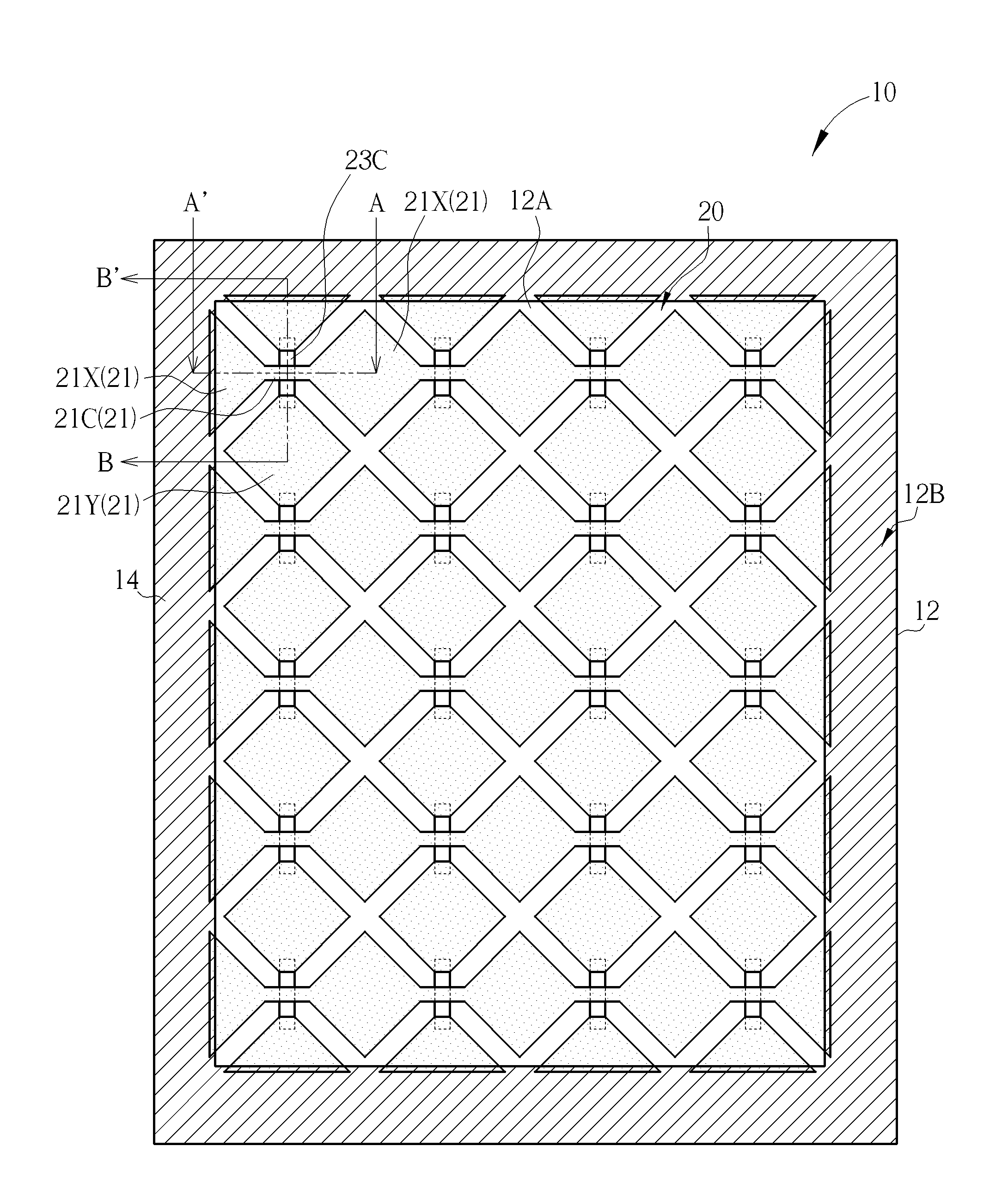
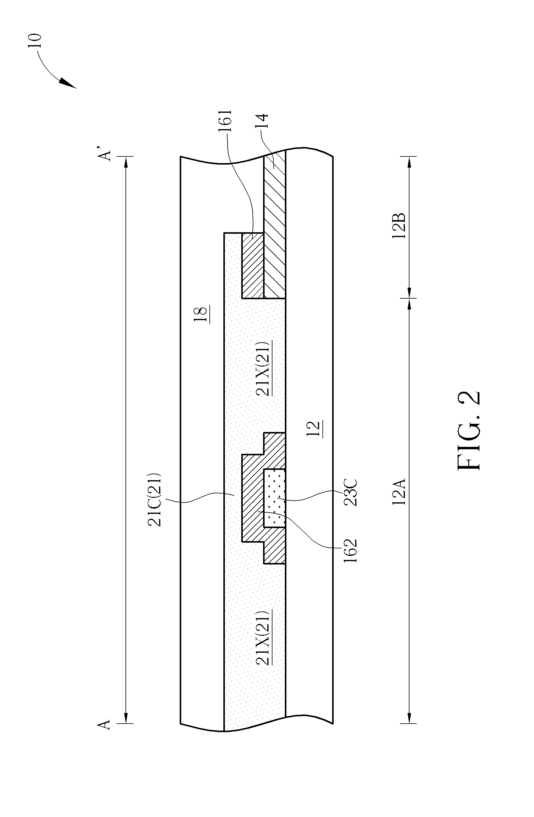
[0030]Please refer to FIGS. 1-3. FIGS. 1-3 are schematic diagrams illustrating a touch panel according to this present invention. FIG. 1 is the schematic diagram illustrating a top view of the touch panel according to the embodiment of the present invention. FIG. 2 is a cross-sectional view diagram taken along a cross-sectional line A-A′ in FIG. 1. FIG. 3 is a cross-sectional view diagram taken along a cross-sectional line B-B′ in FIG. 1. As shown in FIGS. 1-3, the touch panel 10 of this embodiment includes a substrate 12, a decoration layer 14, a touch sensing device 20, and at least one first insulation pattern 161. The substrate 12 may be a hard transparent substrate, such as a glass substrate, or a flexible transparent substrate, such as a plastic substrate, but not limited thereto. The substrate 12 has a light transmissible region 12A and a peripheral region 12B, which surrounds the light transmissible region 12A. The decoration layer 14 is disposed in the peripheral region 12B...
second embodiment
[0035]Please refer to FIGS. 5-6. FIGS. 5-6 are schematic diagrams illustrating a touch panel according to the present invention. FIG. 5 is a schematic diagram illustrating a top view of the touch panel according to this embodiment. FIG. 6 is a cross-sectional view diagram taken along a cross-sectional line C-C′ in FIG. 5. As shown in FIGS. 5-6, in this embodiment, the first patterned transparent sensing layer 21 of the touch panel 30 includes a plurality of transparent sensing electrodes 21P. The transparent sensing electrodes 21P are electrically isolated. The transparent sensing electrodes 21P which locate in the light transmissible region 12A extend to the peripheral region 12B and overlap the decoration layer 14. The first insulation patterns 161 are disposed in the peripheral region 12B on the substrate 12 and interposed between the transparent sensing electrodes 21P and the decoration layer 14. The transparent sensing electrodes 21P do not contact the decoration layer 14. In t...
third embodiment
[0037]Please refer to FIGS. 9-11. FIGS. 9-11 are schematic diagrams illustrating a touch panel according to this present invention. FIG. 9 is a schematic diagram illustrating a top view of the touch panel according to the embodiment of the present invention. FIG. 10 is a cross-sectional view diagram taken along a cross-sectional line E-E′ in FIG. 9. FIG. 11 is a cross-sectional view diagram taken along a cross-sectional line F-F′ in FIG. 9. As shown in FIGS. 9-11, in the touch panel 40 of this embodiment, the touch sensing device 20 is a double-layered transparent electrode structure. Therefore, the touch sensing device 20 includes a first patterned transparent sensing layer 21 and a second patterned transparent layer 22. The first patterned transparent sensing layer 21 includes a plurality of first transparent sensing electrodes 21X and a plurality of first transparent connection lines 21C; any two of the first transparent sensing electrodes 21X adjacent to each other are connected...
PUM
 Abstract
Description
Claims
Application Information
 - R&D
- Intellectual Property
- Life Sciences
- Materials
- Tech Scout
- Unparalleled Data Quality
- Higher Quality Content
- 60% Fewer Hallucinations
Browse by: Latest US Patents, China's latest patents, Technical Efficacy Thesaurus, Application Domain, Technology Topic, Popular Technical Reports.
© 2025 PatSnap. All rights reserved.Legal|Privacy policy|Modern Slavery Act Transparency Statement|Sitemap|About US| Contact US: help@patsnap.com