Antistatic protection structure and reliability improving method of semiconductor panel

A technology for protecting structures and semiconductors, applied in the fields of semiconductor devices, semiconductor/solid-state device manufacturing, semiconductor/solid-state device components, etc., can solve problems such as high reliability risks of semiconductor panels, reduce the risk of short circuits, and improve reliability. Effect

Inactive Publication Date: 2016-10-26
SHANGHAI IRAY TECH
View PDF4 Cites 11 Cited by
  • Summary
  • Abstract
  • Description
  • Claims
  • Application Information

AI Technical Summary

Problems solved by technology

[0008] In view of the above-mentioned shortcomings of the prior art, the purpose of the present invention is to provide an anti-static protection structure of a s

Method used


Image

  • Antistatic protection structure and reliability improving method of semiconductor panel
  • Antistatic protection structure and reliability improving method of semiconductor panel
  • Antistatic protection structure and reliability improving method of semiconductor panel

Examples


Embodiment 1

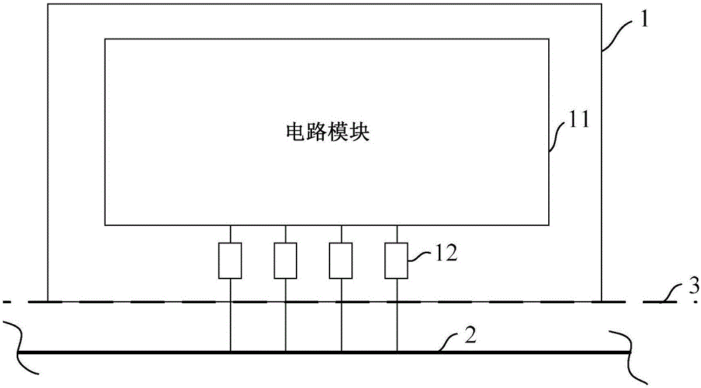
[0048] Such as Figure 4 As shown, the present invention provides an antistatic protection structure of a semiconductor panel, the antistatic protection structure of the semiconductor panel at least includes:

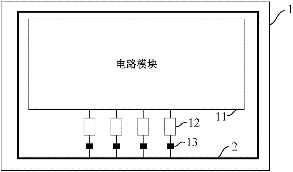
[0049] The anti-static protection ring 2 arranged on the periphery of the circuit area, the circuit area includes a circuit module 11 and a plurality of pads 12 connected to the circuit module 11, each pad 12 is connected to the anti-static protection ring through a short wire 14 respectively. The ring 2 is short-circuit connected; wherein, the part where the antistatic protection ring 2 is connected to each short wire 14 is located outside the cutting line 3 of the semiconductor panel 1, and the upper layer of the short wire 14 is covered with a passivation insulating layer 16, and the semiconductor The passivation insulating layer 16 above the short wires 14 in the panel 1 is provided with a cutout window 13 for exposing the film layer where each short wire is located...

Embodiment 2

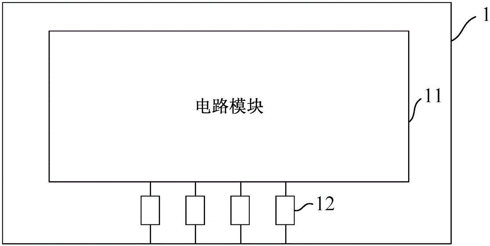
[0059] Such as Figure 5 As shown, the antistatic protection structure of a semiconductor panel is provided in this embodiment, and the difference from Embodiment 1 is that the semiconductor panel 1 is a thin film transistor area array drive panel of a flat panel display; the cut window 13 It is a groove spanning all the short wires 14 ; meanwhile, the part of the antistatic protection ring 2 not connected to each short wire 14 is located outside the semiconductor panel 1 .

[0060] Specifically, when the semiconductor panel 1 is a thin film transistor area array drive panel of a flat panel display, correspondingly, the conductive film layer on the passivation insulating layer 16 has the function of blocking electron radiation, ultraviolet rays and The material of the ITO layer (Indium Tin Oxides, Indium Tin Metal Oxide) with infrared rays can be set according to specific requirements, and will not be repeated here.

[0061] Specifically, such as Figure 5 As shown, the cutt...

Embodiment 3

[0065] Such as Figure 4 ~ Figure 9 As shown, the present invention also provides a method for improving the reliability of a semiconductor panel, and the method for improving the reliability of a semiconductor panel at least includes:

[0066] During the manufacturing process of the semiconductor panel, the anti-static protection structure of the semiconductor panel is prepared, and each point and each film layer of the circuit module is kept at the same potential to avoid electrostatic damage caused by local charge accumulation during the panel manufacturing process.

[0067] Specifically, thin films of different substances are deposited layer by layer on the substrate 15 to form the circuit module 11 and the pads 12 connected thereto in the circuit area. In this embodiment, the substrate 15 is glass. At the same time, if Figure 6 As shown, the short wiring 14 is formed on the substrate 15 between the circuit area and the antistatic protection ring 2, and a passivation ins...


PUM


Abstract

The invention provides an antistatic protection structure and a reliability improving method of a semiconductor panel. The antistatic protection structure comprises an antistatic protection ring, a circuit module and pads, each pad is in short-circuit connection with the antistatic protection ring via a short-circuit line, part, connected with the short-circuit lines, of the antistatic protection ring is positioned at the outer side of a cutting line of the semiconductor panel, and a passivation insulating layer over the short-circuit lines in the semiconductor panel is internally provided with a cut-off window out of which a short-circuit line film layer is exposed. In the manufacture process of the panel, different points of the circuit are kept in the same potential, and static injury is avoided; before completion of the manufacture process of the panel, the short-circuit lines are cut off to disconnect the pads from the antistatic protection ring; and after completion of the manufacture process of the panel, the parts outside the panel of the short-circuit lines are cut to realize dual electrical isolation of the circuit module from the antistatic protection ring. On the premise that a static protection effect is ensured, the reliability of the panel is improved greatly.

Description

technical field [0001] The invention relates to the design field of a thin film transistor area array drive panel of a flat panel display or a thin film transistor area array sensor panel of an X-ray sensor, in particular to an antistatic protection structure of a semiconductor panel and a method for improving reliability. Background technique [0002] The semiconductor panel process is to deposit thin films of different substances on the surface of glass or other flat panels, and pattern them into various circuits to achieve various functions, such as the driving of liquid crystal display panels, the driving of organic light-emitting diode display panels, and X-ray flat panel detection. Sensing function of the sensor panel, etc. However, in the process of semiconductor panel process, since no potential is connected, metal layers on the semiconductor panel or other conductive layers, and between different circuits of the same layer of metal are easily damaged due to the loca...

Claims


Application Information

Patent Timeline
IPC IPC(8): H01L23/60H01L21/02
CPCH01L23/60H01L21/02
Inventor 朱翀煜金利波方志强
Owner SHANGHAI IRAY TECH
Why Eureka
Try Eureka