Insulating substrate, metal-clad laminate, printed wiring board and semiconductor device

a technology of printed wiring boards and substrates, which is applied in the direction of semiconductor/solid-state device details, transportation and packaging, and other domestic articles, can solve the problems of increased susceptibility to warping, increased susceptibility to problems, and decreased reliability, so as to achieve high design freedom and control the direction and degree of warping

Inactive Publication Date: 2013-09-19
SUMITOMO BAKELITE CO LTD
View PDF1 Cites 23 Cited by
  • Summary
  • Abstract
  • Description
  • Claims
  • Application Information

AI Technical Summary

Benefits of technology

[0041]According to the present invention, as a result of at least one fibrous base material layer contained by an insulating substrate being shifted towards a first side or a second side with respect to a reference position of the order corresponding to the fibrous base material layer, and not having any fibrous base material layers shifted in different directions, the insulating substrate and a printed wiring board that uses this insulating substrate are formed either warped outward in the direction in which the fibrous base material layer is shifted or flat, and the direction and degree of warping can be controlled. Thus, by aligning the direction in which the fibrous base material layer contained in the insulating

Problems solved by technology

Consequently, when the thickness of the core substrate is reduced, stress generated by differences in linear coefficients of expansion of each portion surpasses the rigidity of the core substrate, resulting in the problem of increased susceptibility to warping.
If negative warping of the semiconductor device is excessively large, there is increased susceptibility to the occurrence of problems such a defective connections d

Method used


Image

  • Insulating substrate, metal-clad laminate, printed wiring board and semiconductor device
  • Insulating substrate, metal-clad laminate, printed wiring board and semiconductor device
  • Insulating substrate, metal-clad laminate, printed wiring board and semiconductor device

Examples


example 1

1. Production of Metal-Clad Laminate

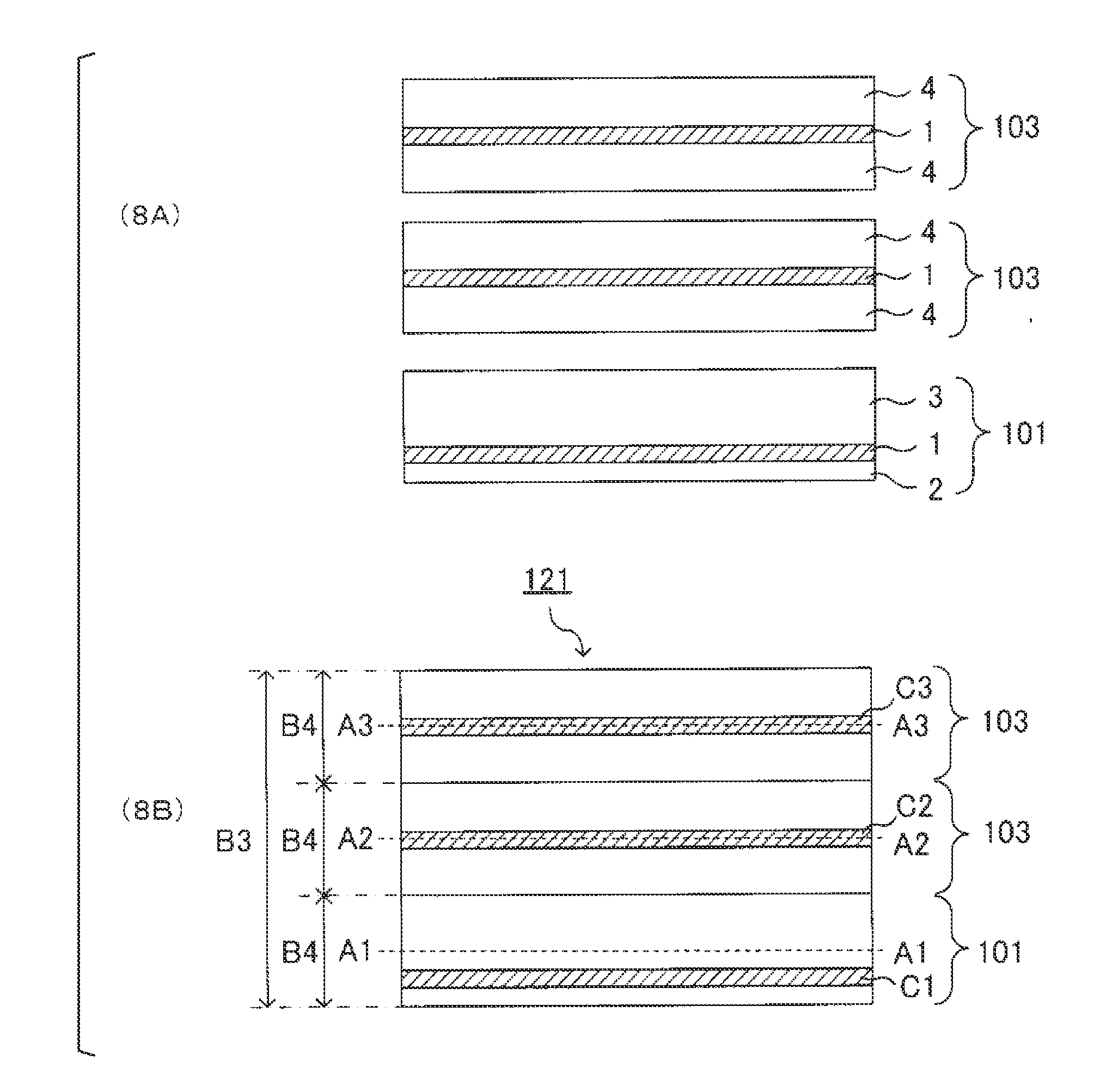
[0243]A 12 μm copper foil (Mitsui Mining and Smelting Co., Ltd., 3EC-VLP Foil) was superimposed on both sides of Prepreg 1 followed by subjecting to heated pressure molding for 2 hours at 220° C. and 3 MPa to obtain a metal-clad laminate. The core layer (portion composed of an insulating substrate) of the resulting metal-clad laminate had the same layer composition as that of the insulating substrate 111 of FIG. 1A, had a layer composition obtained by laminating in order starting from a first side the resin layer r1, the fibrous base material layer C1 and the resin layer r2, the thicknesses of each layer were 3 μm for r1, 28 μm for C1 and 9 μm for r2, and the aforementioned core layer was such that the fibrous base material layer C1 was shifted towards the resin layer r1 with respect to a reference position. In addition, the total thickness (B3) of the core layer was 40 μm.

[0244]The ratio of B5 / B6 of the aforementioned core layer was 0.33 since th...

examples 2 to 5

[0254]Printed wiring boards and semiconductor devices of Examples 2 to 5 were produced in the same manner as Example 1 with the exception of respectively producing metal-clad laminates using Prepreg 2 in Example 2, Prepreg 3 in Example 3, Prepreg 5 in Example 4 and Prepreg 6 in Example 5, and using the resulting metal-clad laminates as core substrates. In the core substrates of Examples 2 to 5, the fibrous base material layers were shifted towards the first side with respect to a reference position. Furthermore, semiconductor elements were mounted on printed wiring boards for a semiconductor device so that the side on the opposite side from the side in the direction in which the fibrous base material layer of the core substrate is shifted is the side where the semiconductor element is mounted.

example 6

1. Production of Metal-Clad Laminate

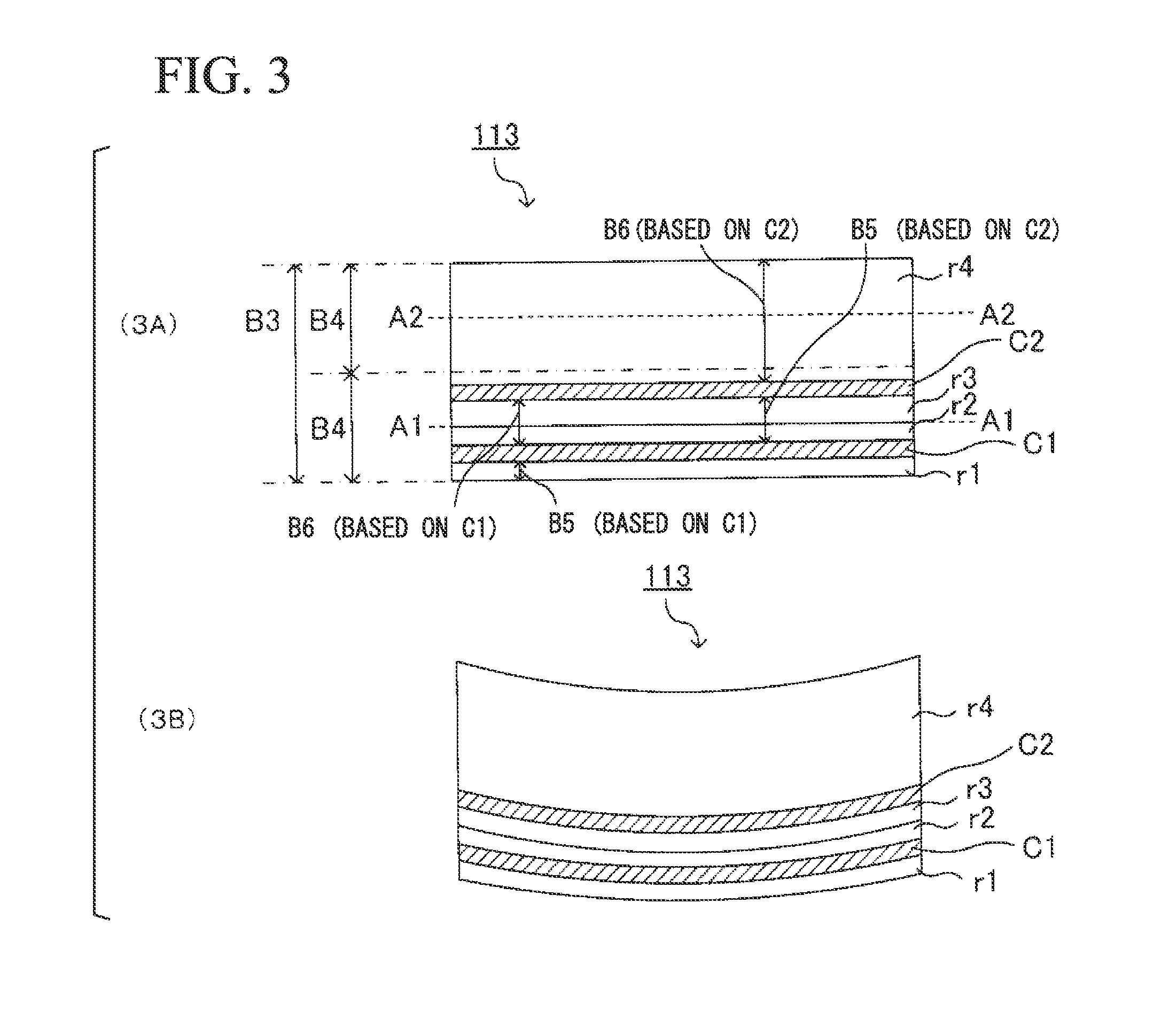
[0255]A total of three prepregs were laminated in the order of Prepreg 10, Prepreg 10 and Prepreg 4 so that the second resin layer of Prepreg 4 was on the side of Prepreg 10 and the first resin layer was on the side of an air layer, 12 μm copper foil (Mitsui Mining and Smelting Co., Ltd., 3EC-VLP Foil) was superimposed on both sides of the resulting laminate followed by subjecting to heated pressure molding for 2 hours at 220° C. and 3 MPa to obtain a metal-clad laminate. The core layer (portion composed of an insulating substrate) of the resulting metal-clad laminate had the same layer composition as that of the insulating substrate 115 of FIG. 5A, and had a layer composition obtained by laminating in order starting from a first side the resin layer r1, the fibrous base material layer C1, the resin layers r2 and r3, the fibrous base material layer C2, the resin layers r4 and r5, the fibrous base material layer C3 and the resin layer r6. The thick...


PUM

PropertyMeasurementUnit
Thicknessaaaaaaaaaa
Thicknessaaaaaaaaaa
Sizeaaaaaaaaaa

Abstract

The present invention provides: an insulating substrate or metal-clad laminate able to sufficiently reduce or prevent negative warping of a semiconductor device; a printed wiring board that uses the insulating substrate or metal-clad laminate; and a semiconductor device. The insulating substrate is composed of a cured product of a laminate including one or more fibrous base material layers and two or more resin layers, in which the outermost layers on both sides is the resin layers. At least one of the fibrous base material layers is shifted towards the first side or a second side on the opposite side thereof with respect to the reference position, namely the dividing position at which a total thickness of the insulating substrate is equally divided by the number of the fibrous base material layers and each divided region having the thickness is further equally divided by two. The fibrous base material layers are not shifted in different directions. It is possible to produce a printed wiring board by using, as a core substrate, a metal-clad laminate containing the insulating substrate. Also, it is possible to produce a semiconductor device by mounting a semiconductor element onto the printed wiring board.

Description

TECHNICAL FIELD[0001]The present invention relates to an insulating substrate and a metal-clad laminate serving as core substrates for producing a printed wiring board, a printed wiring board that uses the insulating substrate or the metal-clad laminate, and a semiconductor device.[0002]The present application claims priority based on Japanese Patent Application No. 2010-258172, filed in Japan on Nov. 18, 2010, and Japanese Patent Application No. 2011-209540, filed in Japan on Sep. 26, 2011, the contents of which are incorporated herein by reference.BACKGROUND ART[0003]Semiconductor devices (semiconductor packages) used in electronic equipment are continuing to become increasingly compact, have higher density, and demonstrate increasingly sophisticated functions, and examples of package forms include package-on-package (POP), system-in-package (SIP) and flip chip ball grid arrays (FCBGA). Accompanying the increasingly compact sizes and high densities of these semiconductor devices, ...

Claims


Application Information

Patent Timeline
IPC IPC(8): H05K1/03
CPCB32B5/02Y10T428/2495B32B2457/08H01L23/49822H01L23/49827H05K1/036H05K1/0366H05K2201/029H01L2224/16227H01L2224/73204H01L2924/15311H05K1/038H01L2924/01322B32B2307/734Y10T428/24967H01L2224/16225H05K3/4602H01L2924/00H01L2924/00014H01L2224/0401B32B27/12B32B15/08H05K3/46H01L23/12
Inventor ONOZUKA, IJI
Owner SUMITOMO BAKELITE CO LTD
Why Eureka
Try Eureka