
Method for Producing a Conversion Lamina and Conversion Lamina

a technology of conversion laminae and laminae, which is applied in the direction of electrical equipment, semiconductor devices, solid-state devices, etc., can solve the problem that the high layer thickness of the conversion laminae cannot be achieved by conventional production methods, and achieve the effect of improving reproducibility, high layer thickness, and improving edge accuracy

Active Publication Date: 2013-10-31
OSRAM OLED
View PDF4 Cites 0 Cited by
  • Summary
  • Abstract
  • Description
  • Claims
  • Application Information

AI Technical Summary

Benefits of technology

The invention relates to a method of producing a conversion lamina with improved reproducibility and edge accuracy. The resulting conversion lamina has a high layer thickness.

Problems solved by technology

Conversely, owing to their small thickness of at most 40 μm, conventionally used screens are limited thereto, so that high layer thicknesses of the conversion laminae cannot be achieved by conventional production methods.

Method used


Image

  • Method for Producing a Conversion Lamina and Conversion Lamina
  • Method for Producing a Conversion Lamina and Conversion Lamina
  • Method for Producing a Conversion Lamina and Conversion Lamina

Examples


Embodiment Construction

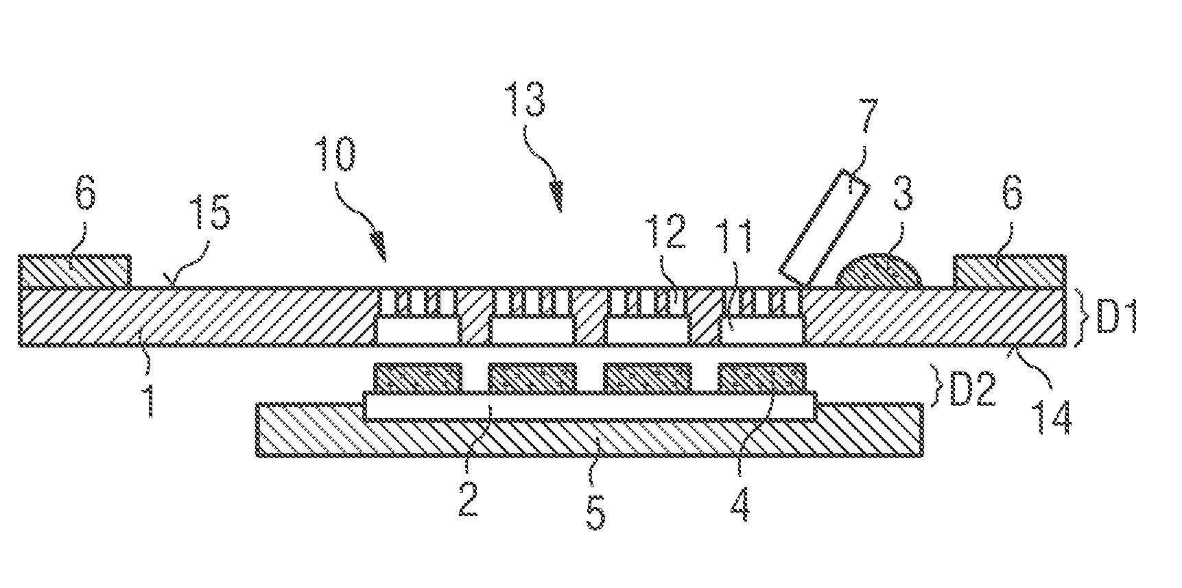
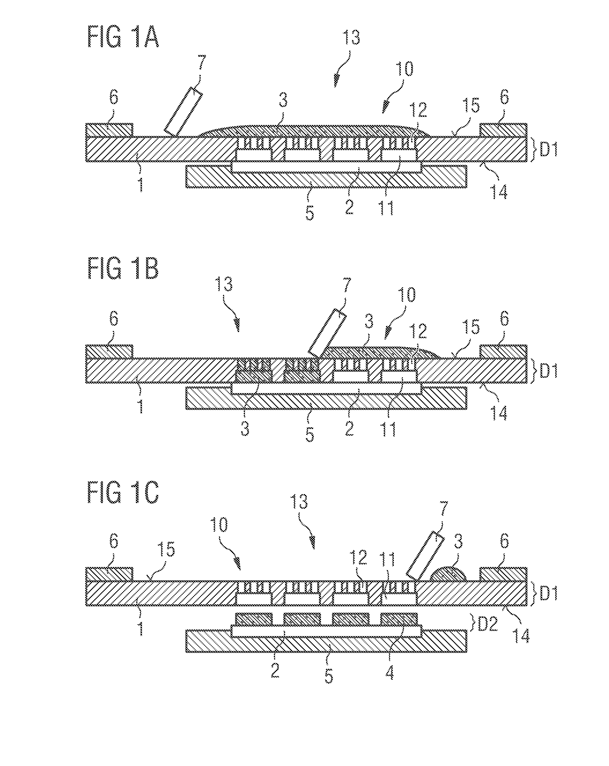
[0045]In FIGS. 1A to 1C, method steps for the production of a multiplicity of conversion laminae are shown. Conversion laminae produced in such a way are suitable in particular for use in combination with radiation-emitting semiconductor components, for example, LEDs. In this case, the conversion laminae are suitable for converting radiation emitted by the radiation-emitting semiconductor component at least partially into radiation of a another wavelength, so that a semiconductor component comprising a conversion lamina arranged thereon has mixed radiation consisting of emitted radiation and converted radiation. The conversion laminae produced are in this case arranged directly after a radiation exit side of the semiconductor component, for example, directly on a radiation exit surface.

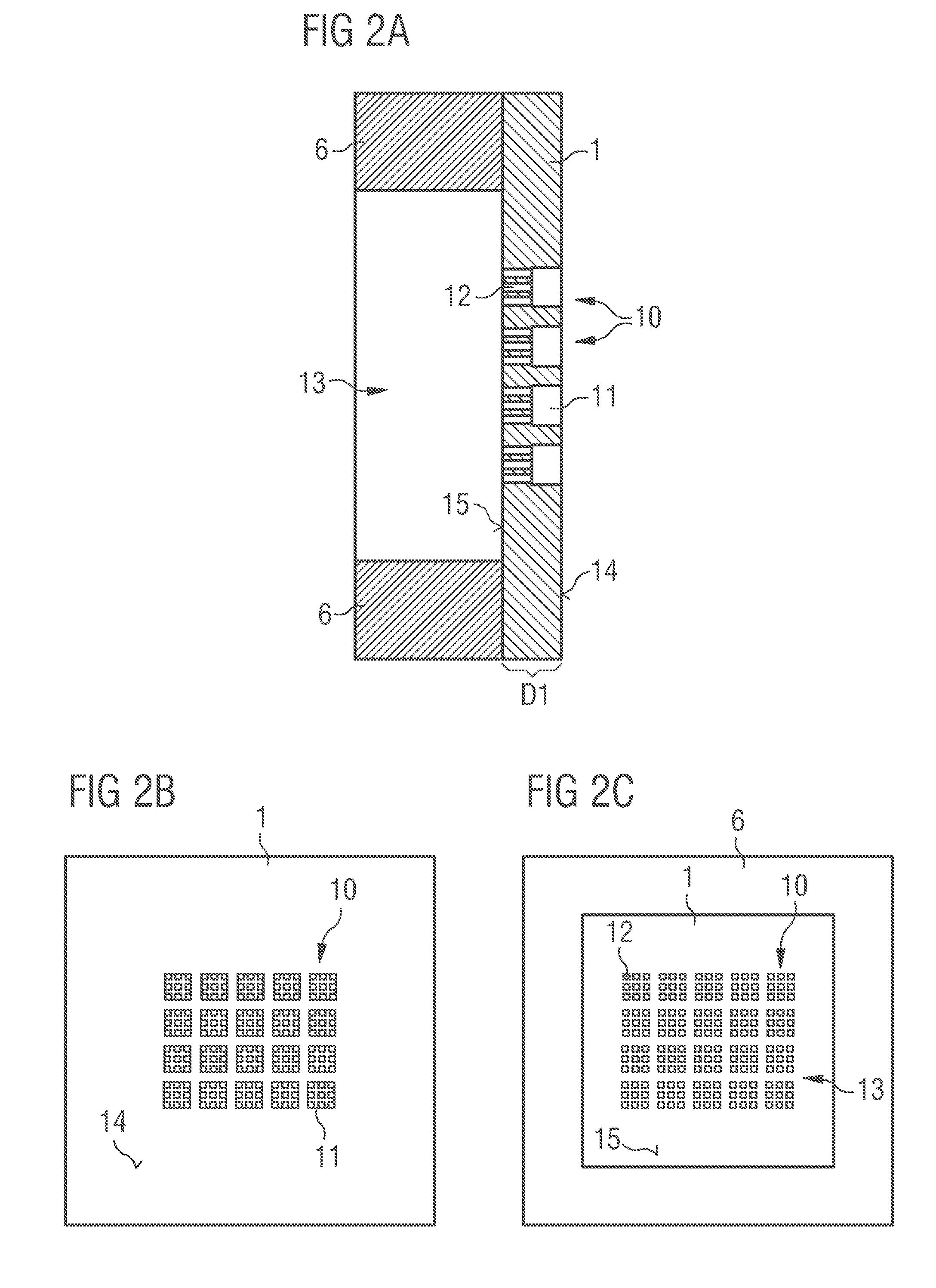
[0046]In order to produce the conversion laminae, a template 1 is used in particular. The template 1 has a thickness D1 in a range of between 80 μm and 150 μm, preferably between 100 μm and 110 μm. Th...


PUM


Abstract

A method for producing at least one conversion lamina for a radiation-emitting semiconductor component is specified. A base material including a conversion substance contained therein is applied to a substrate by means of a double-layered stencil. Furthermore, a conversion lamina for a radiation-emitting semiconductor component includes a base material and a conversion substance embedded therein. The thickness of the conversion lamina is in a range of between 60 μm and 170 μm inclusive.

Description

[0001]This patent application is a national phase filing under section 371 of PCT / EP2011 / 066905, filed Sep. 28, 2011, which claims the priority of German patent application 10 2010 049 312.0, filed Oct. 22, 2010, each of which is incorporated herein by reference in its entirety.TECHNICAL FIELD[0002]The invention relates to a method for producing a conversion lamina for a radiation-emitting semiconductor component. The invention furthermore relates to a conversion lamina for a radiation-emitting semiconductor component.BACKGROUND[0003]Conventionally, conversion laminae are produced inter alia by means of a screen printing method. In this case, the layer thickness of the conversion laminae is controlled by selecting screens with masks of differing thickness. However, the layer thicknesses of conversion laminae produced in this way are limited to about 40 μm in the screen printing method. In the case of conversion laminae which are produced by means of a screen printing method, the con...

Claims


Application Information

Patent Timeline
Patent Type & Authority Applications(United States)
IPC IPC(8): H01L33/44H10K99/00
CPCH01L33/44H01L33/50H01L33/48H01L21/4867H01L21/56H10K85/141H01L33/502
Inventor RICHTER, MARKUS
Owner OSRAM OLED
Learn More