Systems and methods of automatically detecting failure patterns for semiconductor wafer fabrication processes

a technology of automatic detection and failure pattern, applied in the direction of individual semiconductor device testing, semiconductor/solid-state device testing/measurement, instruments, etc., can solve the problems of inability to detect failure patterns, and inability to achieve high yield

Active Publication Date: 2013-10-31
TAIWAN SEMICON MFG CO LTD
View PDF0 Cites 24 Cited by
  • Summary
  • Abstract
  • Description
  • Claims
  • Application Information

AI Technical Summary

Problems solved by technology

However, despite the sophistication of semiconductor wafer fabrication facilities and expense of semiconductor manufacturing tools, achieving a high yield remains a difficult accomplishment.
For example, the natural variation inherent in processes performed in semiconductor fabrication facilities, tool function changes or drift, inadequate sacrificial film removal, tool imperfections, contamination, and / or tool miscalibration are all challenges facing semiconductor fabrication facilities that can cause unacceptable levels of chip failures.
These non-systematic processes are labor-intensive, time-consuming, limited to small sub-sets of the high volume of semiconductor wafers that are manufactured daily and will be unable to meet Giga Fab and future 450 mm targets.

Method used


Image

  • Systems and methods of automatically detecting failure patterns for semiconductor wafer fabrication processes
  • Systems and methods of automatically detecting failure patterns for semiconductor wafer fabrication processes
  • Systems and methods of automatically detecting failure patterns for semiconductor wafer fabrication processes

Examples


Embodiment Construction

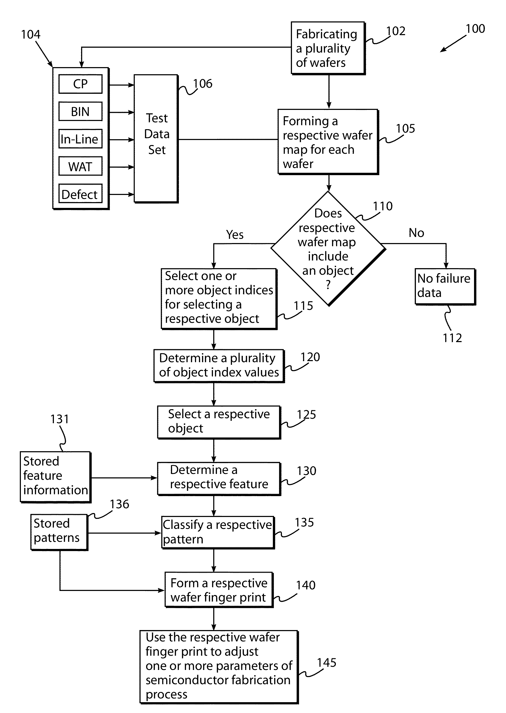
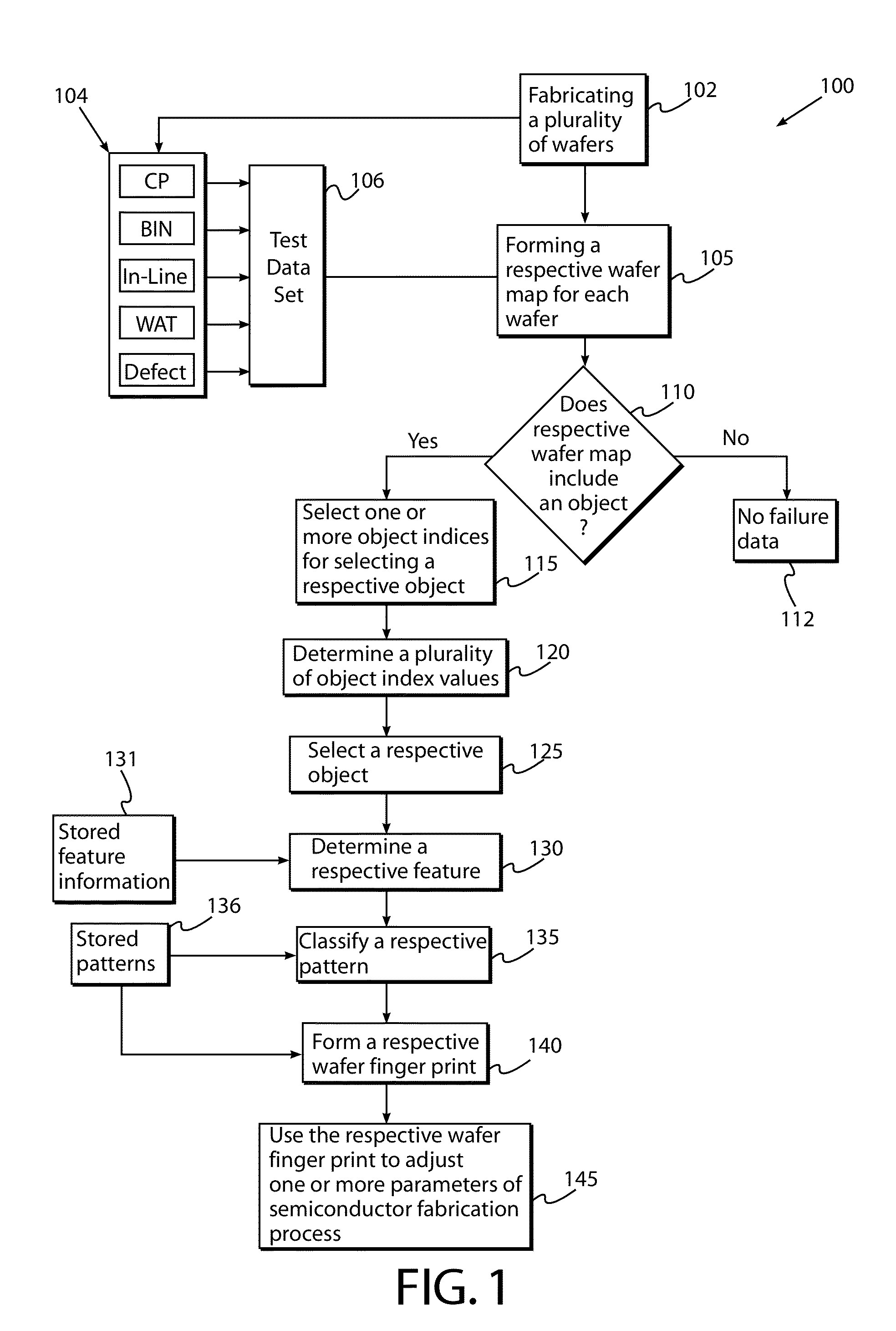
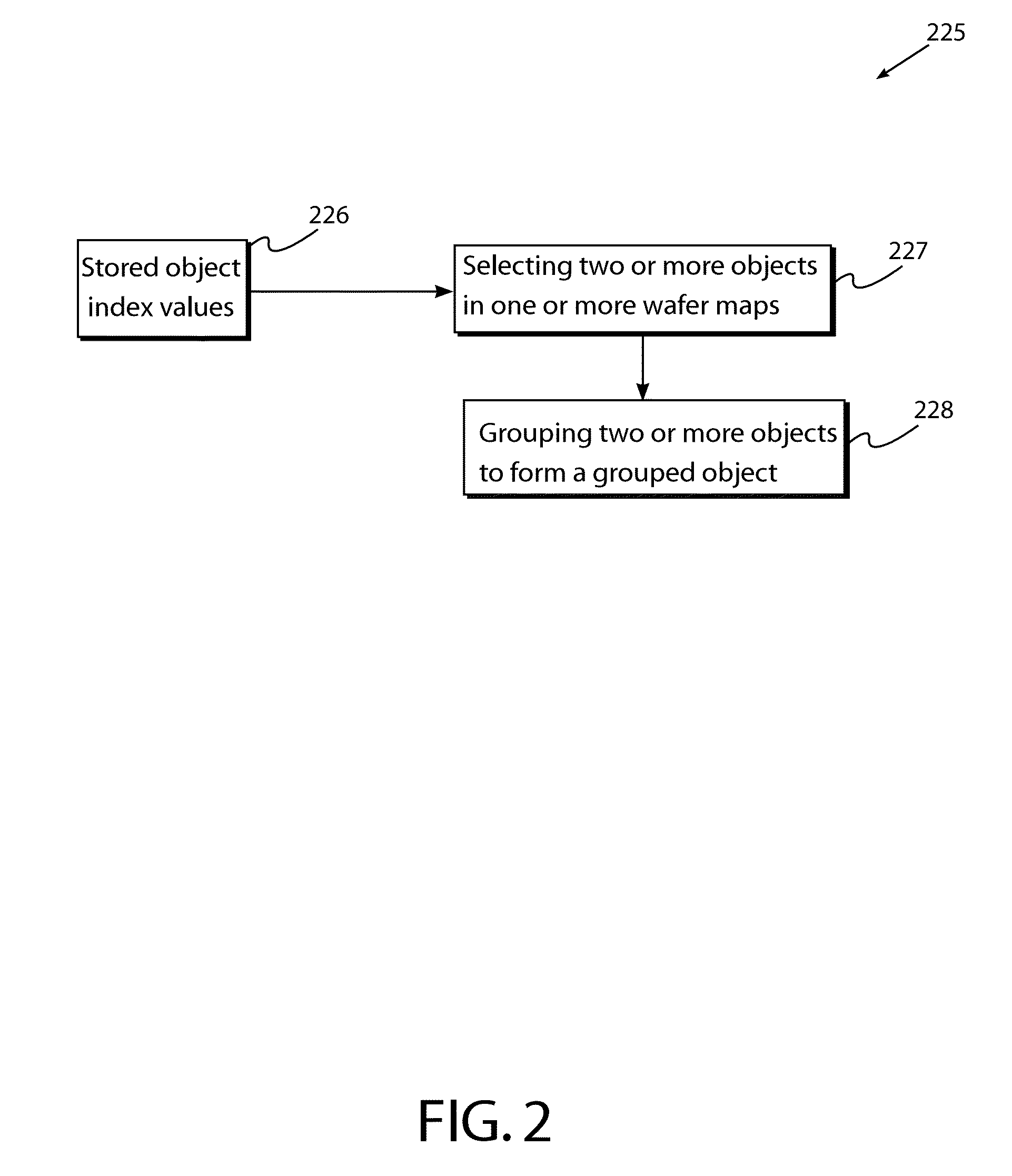
[0020]With reference to the Figures, where like elements have been given like numerical designations to facilitate an understanding of the drawings, the various embodiments of a system and a method of automatically detecting failure patterns for a semiconductor wafer fabrication process are described. The figures are not drawn to scale.

[0021]The following description is provided as an enabling teaching of a representative set of examples. Those skilled in the art will recognize that many changes can be made to the embodiments described herein while still obtaining beneficial results. It will also be apparent that some of the desired benefits discussed below can be obtained by selecting some of the features or steps discussed herein without utilizing other features or steps. Accordingly, those who work in the art will recognize that many modifications and adaptations, as well as subsets of the features and steps described herein are possible and can even be desirable in certain circu...


PUM


Abstract

A system and method of automatically detecting failure patterns for a semiconductor wafer process is provided. The method includes receiving a test data set collected from testing a plurality of semiconductor wafers, forming a respective wafer map for each of the wafers, determining whether each respective wafer map comprises one or more respective objects, selecting the wafer maps that are determined to comprise one or more respective objects, selecting one or more object indices for selecting a respective object in each respective selected wafer map, determining a plurality of object index values in each respective selected wafer map, selecting an object in each respective selected wafer map, determining a respective feature in each of the respective selected wafer, classifying a respective pattern for each of the respective selected wafer maps and using the respective wafer fingerprints to adjust one or more parameters of the semiconductor fabrication process.

Description

FIELD[0001]The present disclosure is directed generally to semiconductor wafer fabrication processes and more particularly to systems and methods to analyze failures in semiconductor wafer fabrication processes.DESCRIPTION OF THE RELATED ART[0002]Integrated circuits are produced by a plurality of complex semiconductor fabrication processes in a semiconductor wafer fabrication facility. Maintaining a high yield in semiconductor fabrication processes continues to be a critical factor in reducing the costs of device fabrication. However, despite the sophistication of semiconductor wafer fabrication facilities and expense of semiconductor manufacturing tools, achieving a high yield remains a difficult accomplishment. For example, the natural variation inherent in processes performed in semiconductor fabrication facilities, tool function changes or drift, inadequate sacrificial film removal, tool imperfections, contamination, and / or tool miscalibration are all challenges facing semicondu...

Claims


Application Information

Patent Timeline
Patent Type & Authority Applications(United States)
IPC IPC(8): H01L21/66G06F19/00
CPCH01L22/20H01L22/10H01L22/12H01L22/14H01L2924/0002H01L2924/00
Inventor CHEN, JUI-LONGCHAO, HUI-YUNTSEN, YEN-DIMOU, JONG-I
Owner TAIWAN SEMICON MFG CO LTD
Why Eureka
Try Eureka