

Semiconductor package and method of fabricating the same
a technology of semiconductor chips and semiconductor components, applied in the direction of semiconductor devices, semiconductor/solid-state device details, electrical devices, etc., can solve the problems of adversely affecting the positional accuracy of semiconductor chips, and achieve the effect of preventing serious warpage and improving product yield
- Summary
- Abstract
- Description
- Claims
- Application Information
AI Technical Summary
Benefits of technology
Problems solved by technology
Method used
Image

Examples
Embodiment Construction
[0032]The following illustrative embodiments are provided to illustrate the disclosure of the present invention, these and other advantages and effects can be apparent to those in the art after reading this specification.
[0033]It should be noted that all the drawings are not intended to limit the present invention. Various modification and variations can be made without departing from the spirit of the present invention. Further, terms such as “first”, “second”, “on”, “a” etc. are merely for illustrative purpose and should not be construed to limit the scope of the present invention.
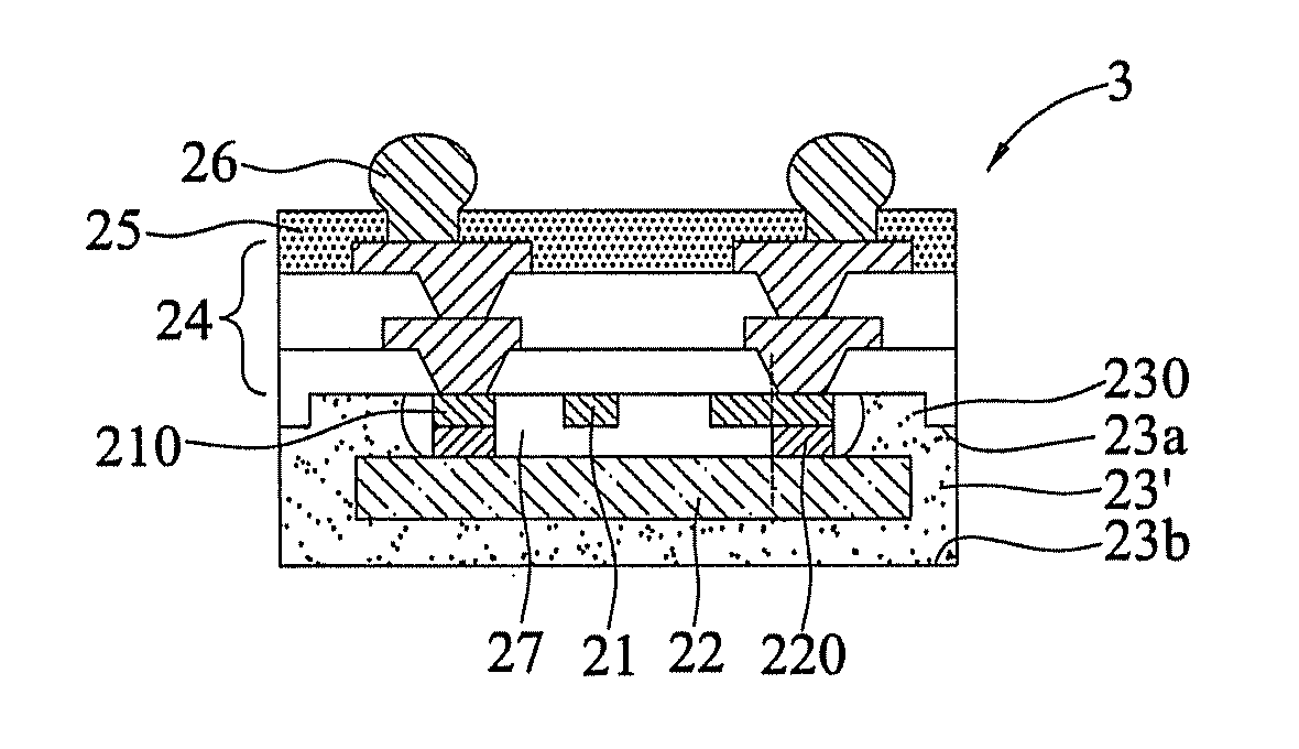
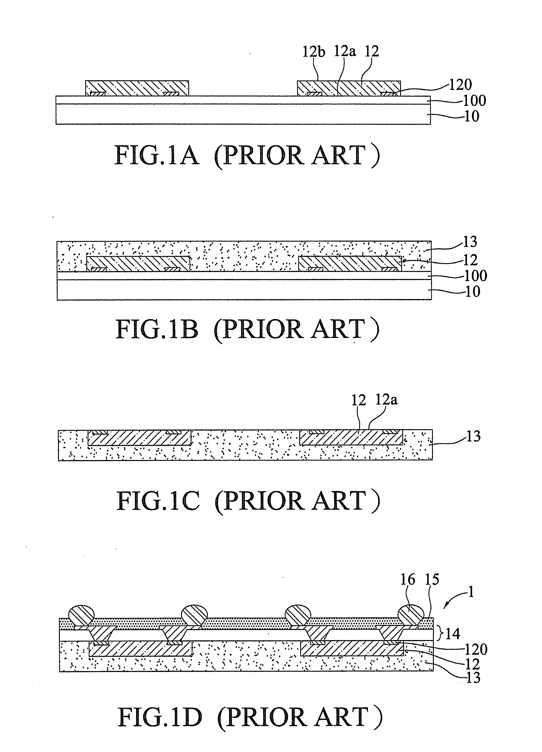
[0034]FIGS. 2A to 2F are schematic cross-sectional views showing a semiconductor package 2 and a method of fabricating the same according to a first embodiment of the present invention.
[0035]Referring to FIG. 2A, a patterned metal layer 21 is formed on a carrier 20 and then a plurality of adhesive bodies 27 are formed on the carrier 20 to encapsulate the patterned metal layer 21. The adhesive bodies 27 s...
PUM
 Abstract
Description
Claims
Application Information