Eureka AIR delivers breakthrough ideas for toughest innovation challenges, trusted by R&D personnel around the world.

Method for fabricating capacitor of semiconductor device

Active Publication Date: 2014-01-02
SK HYNIX INC
View PDF1 Cites 2 Cited by
  • Summary
  • Abstract
  • Description
  • Claims
  • Application Information

AI Technical Summary

Benefits of technology

The present invention provides a method for making a capacitor in a semiconductor device that can ease the process of opening and controlling the shape of the openings without, in some cases, requiring a separate etch process. This can make it easier to control the performance of the capacitor in the device and improve its overall efficiency.

Problems solved by technology

As the integration degree of semiconductor devices increases rapidly, technical difficulty increases as well.
Thus, the above-mentioned problem becomes even worse.

Method used


Image

  • Method for fabricating capacitor of semiconductor device
  • Method for fabricating capacitor of semiconductor device
  • Method for fabricating capacitor of semiconductor device

Examples


Embodiment Construction

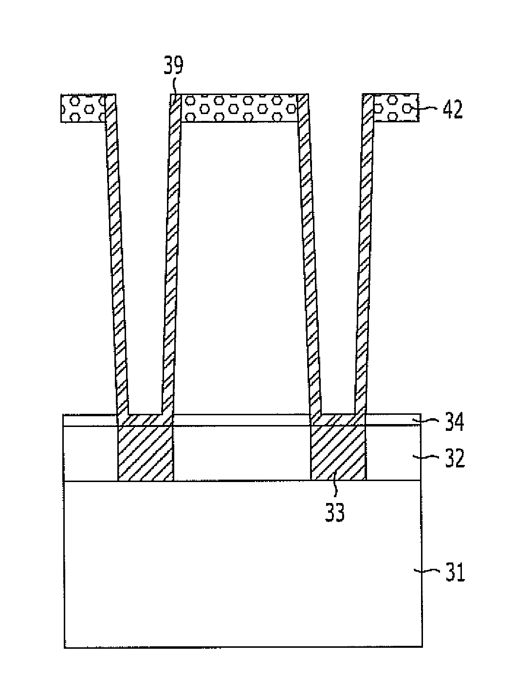
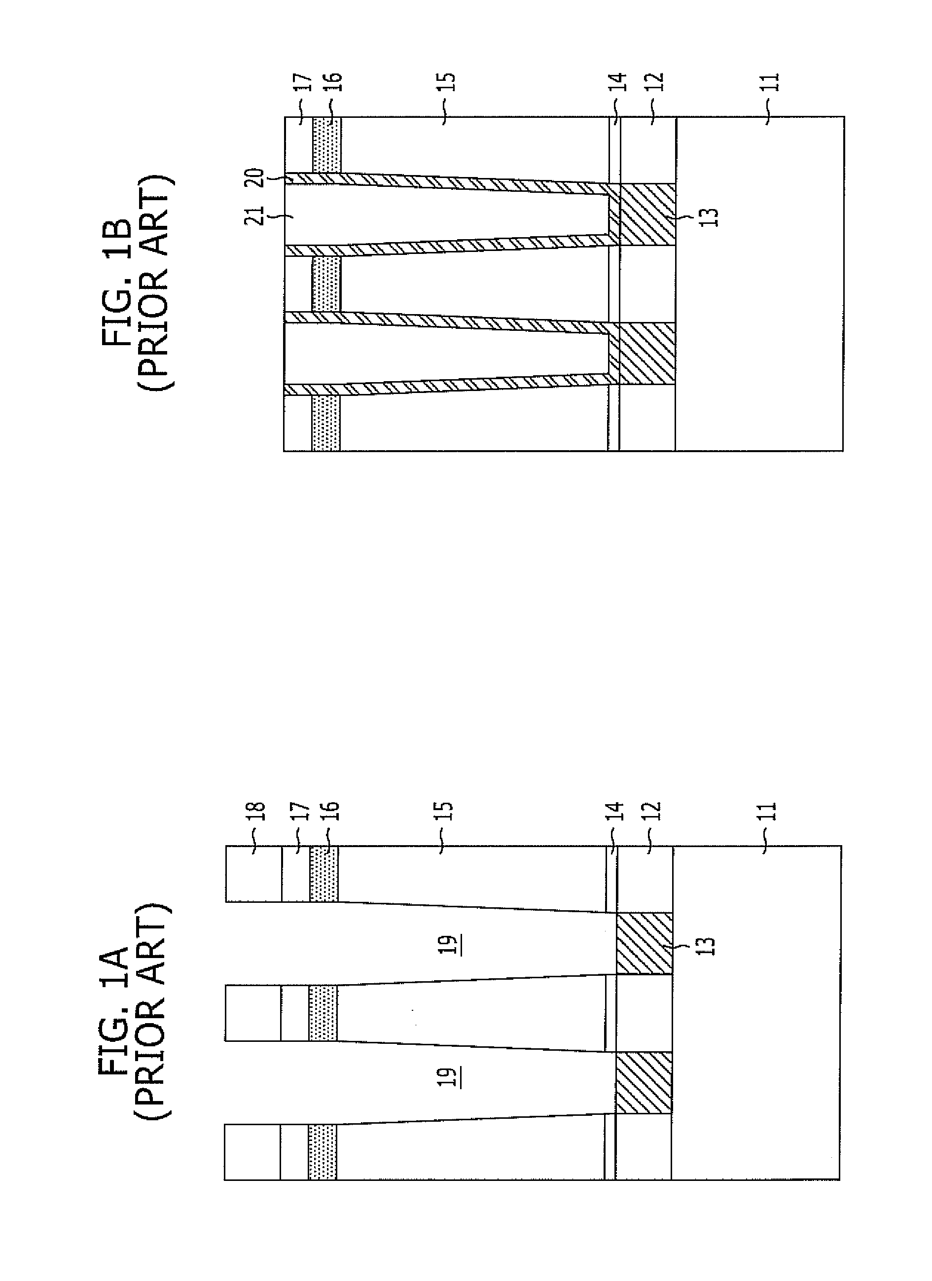
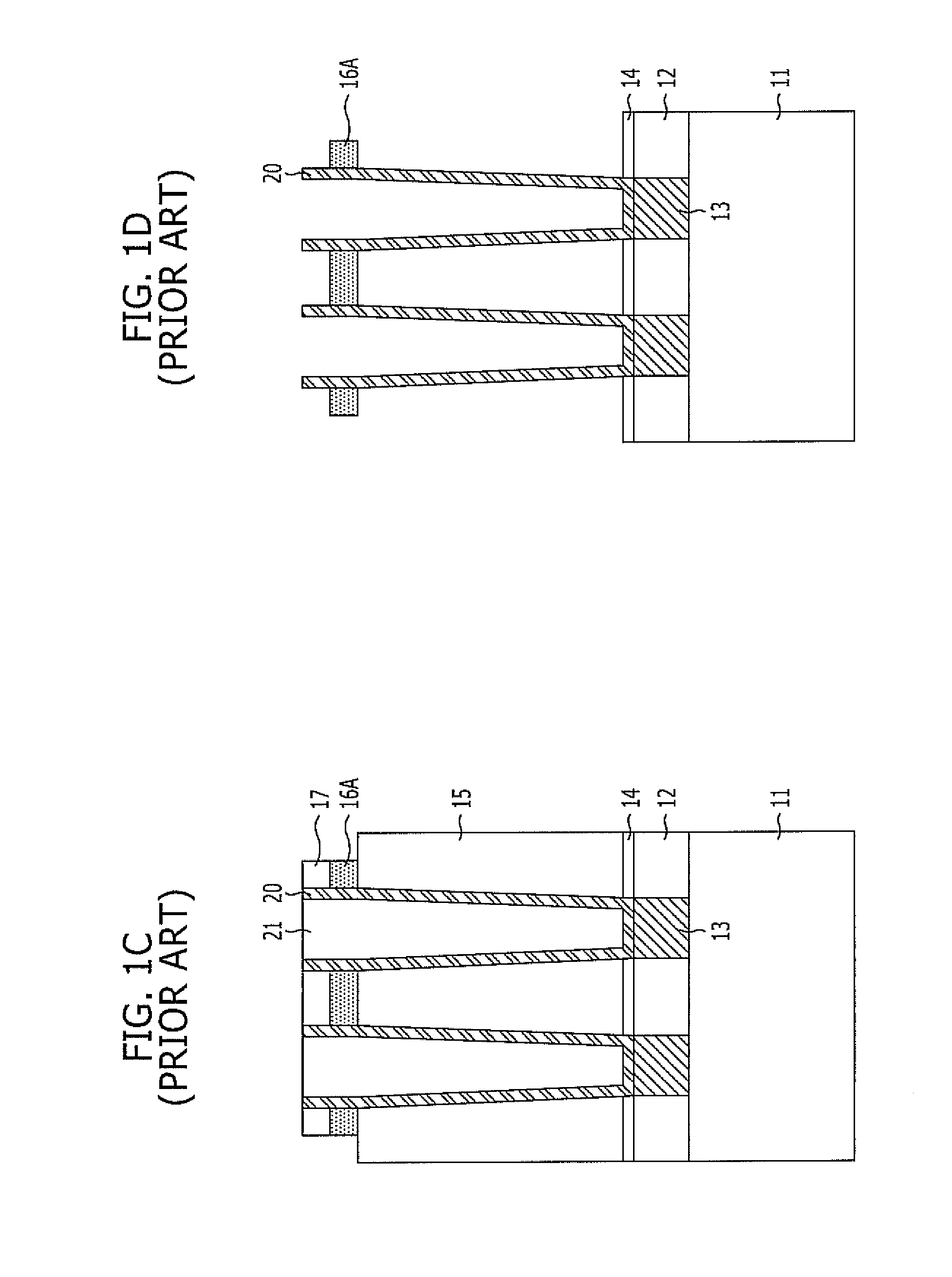
[0022]Exemplary embodiments of the present invention will be described below in more detail with reference to the accompanying drawings. The present invention may, however, be embodied in different forms and should not be construed as limited to the embodiments set forth herein. Rather, these embodiments are provided so that this disclosure will be thorough and complete, and will fully convey the scope of the present invention to those skilled in the art. Throughout the disclosure, like reference numerals refer to like parts throughout the various figures and embodiments of the present invention.

[0023]The drawings are not necessarily to scale and in some instances, proportions may have been exaggerated in order to clearly illustrate features of the embodiments. It should be readily understood that the meaning of “on” and “over” in the present disclosure should be interpreted in the broadest manner such that “on” not only means “directly on” something but also include the meaning of ...


PUM


Abstract

A method for fabricating a capacitor of a semiconductor device includes forming a mold layer over a substrate, forming a plurality of preliminary openings by selectively etching the mold layer, forming a plurality of openings where each opening is formed to have a given linewidth by forming a sacrificial layer on sidewalls of the preliminary openings, and forming a plurality of storage nodes in the plurality of openings.

Description

CROSS-REFERENCE TO RELATED APPLICATIONS[0001]The present application claims priority of Korean Patent Application No. 10-2012-0071152, filed on Jun. 29, 2012, which is incorporated herein by reference in its entirety.BACKGROUND[0002]1. Field[0003]Exemplary embodiments of the present invention relate to a semiconductor designing technology, and more particularly, to a method for fabricating a capacitor of a semiconductor device.[0004]2. Description of the Related Art[0005]As the integration degree of semiconductor devices increases rapidly, technical difficulty increases as well. For example, a Dynamic Random Access Memory (DRAM) device necessarily requires a process for forming storage nodes having a high aspect ratio in order to provide a capacitor of a required capacitance due to design shrinkage. The storage node process is a process of forming hole-type openings by etching a mold layer and then forming storage nodes in the openings.[0006]FIGS. 1A to 1D are cross-sectional views ...

Claims


Application Information

Patent Timeline
IPC IPC(8): H01L21/02
CPCH01L28/91H10B12/033H10B99/00H10B12/00
Inventor LIM, SUNG-WONYEOM, SEUNG-JINLEE, HYO-SEOK
Owner SK HYNIX INC
Why Eureka
Eureka Blog
Learn More