Digital to Analog Converter and Source Driver Chip Thereof
- Summary
- Abstract
- Description
- Claims
- Application Information
AI Technical Summary
Benefits of technology
Problems solved by technology
Method used
Image
Examples
Embodiment Construction
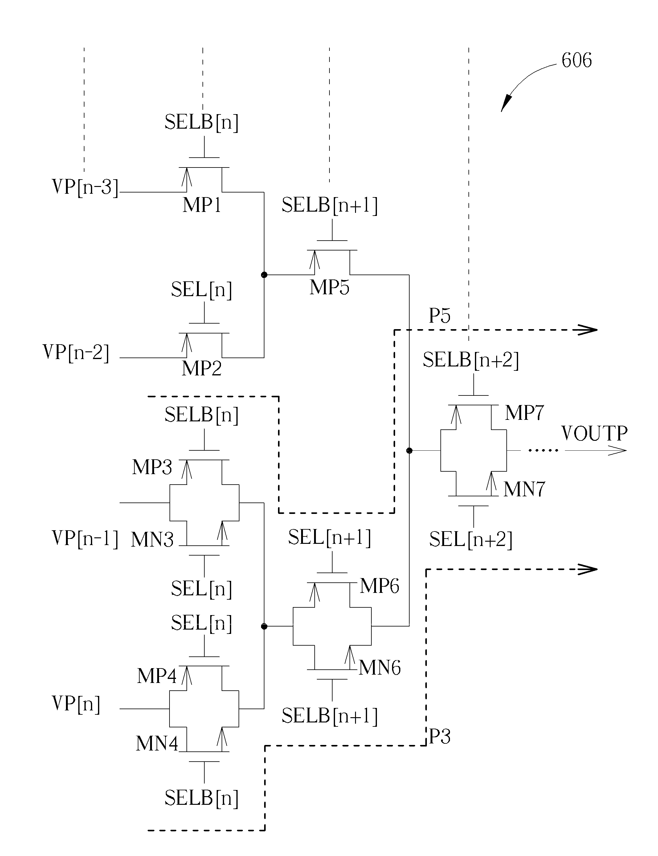
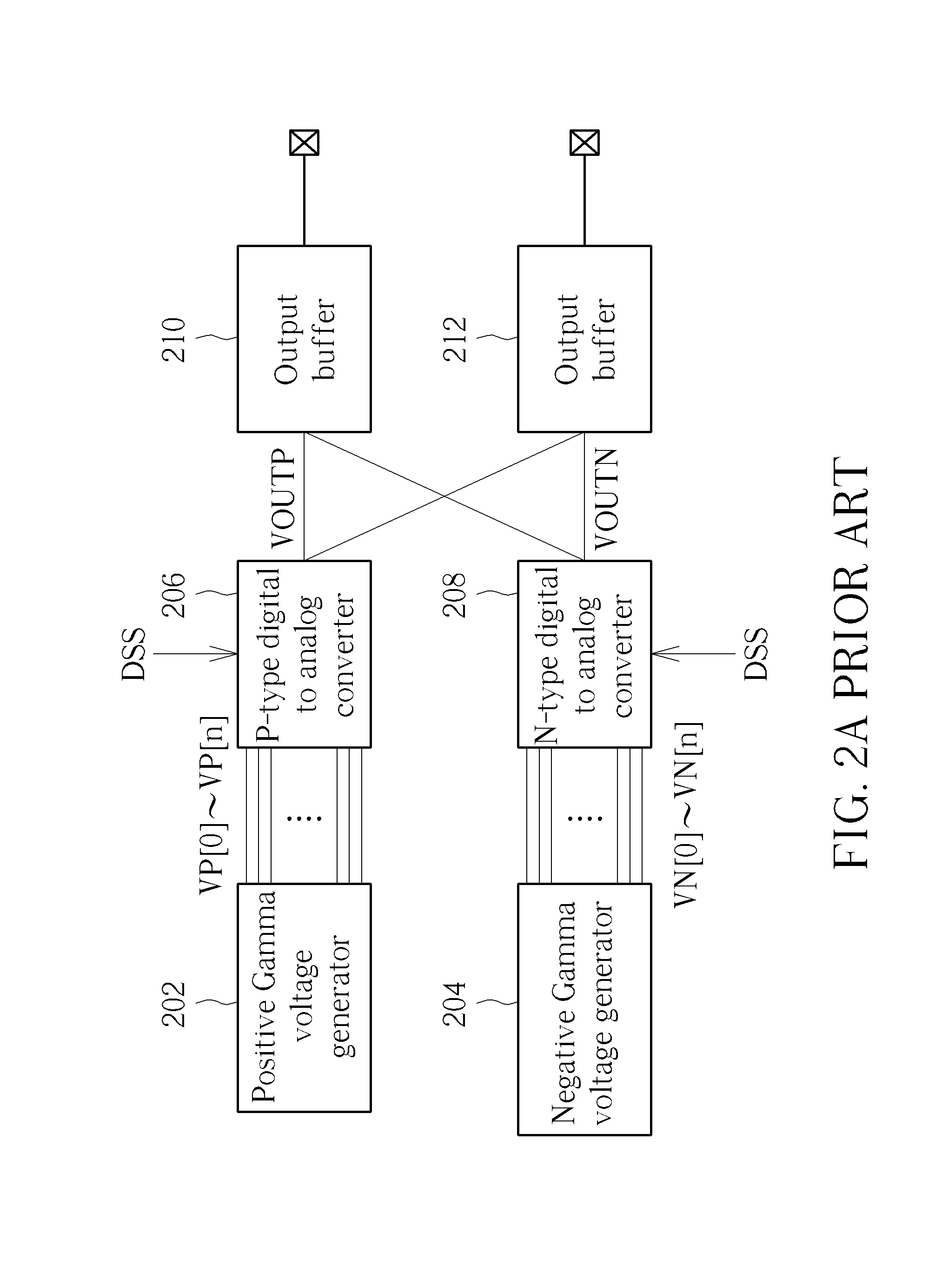
[0024]Please refer to FIG. 3A and FIG. 3B, which are schematic diagrams of partial circuits of a p-type digital to analog converter 306 and an n-type digital to analog converter 308 utilized for replacing the p-type digital to analog converter 206 and the n-type digital to analog converter 208 in FIG. 2A according to an embodiment of the present invention. The p-type digital to analog converter 306 is partially similar to the p-type digital to analog converter 206, and hence elements and signals with similar functions are denoted by the same symbols. The main difference between the p-type digital to analog converter 306 and the p-type digital to analog converter 206 is that a transmission path P2 corresponding to a receiving terminal receiving the positive Gamma voltage VP[n] closest to the middle voltage VDDA / 2 among the positive Gamma voltages VP[0]˜VP[n] (i.e. the minimal of the positive Gamma voltages VP[0]˜VP[n]) has lower on-resistance than transmission paths corresponding to ...
PUM
 Abstract
Description
Claims
Application Information


