Image scanning device and image forming apparatus

a scanning device and image technology, applied in the direction of electrical devices,pictoral communication, etc., can solve the problem of inefficient black-level correction data

a scanning device and image technology, applied in the direction of electrical devices,pictoral communication, etc., can solve the problem of inefficient black-level correction data

US20140029065A1Active Publication Date: 2014-01-30RICOH KK

Image

  • Image scanning device and image forming apparatus
  • Image scanning device and image forming apparatus
  • Image scanning device and image forming apparatus

Examples


first embodiment

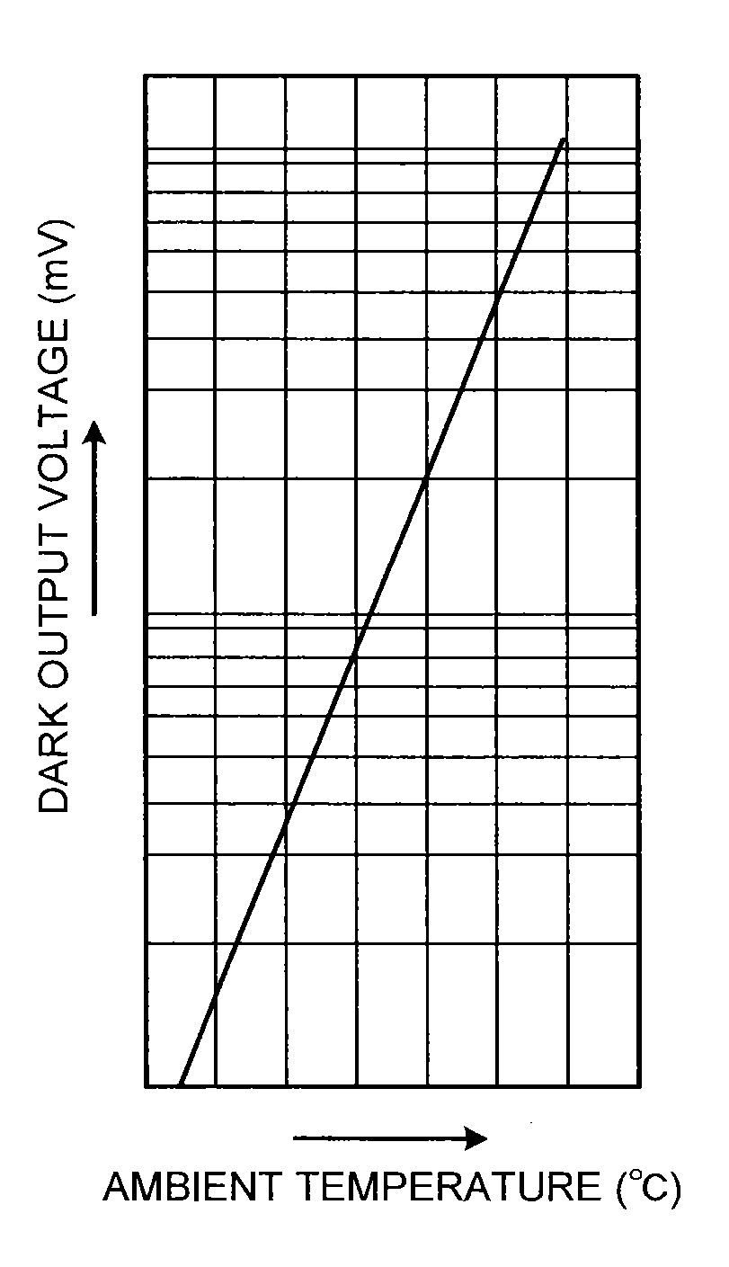
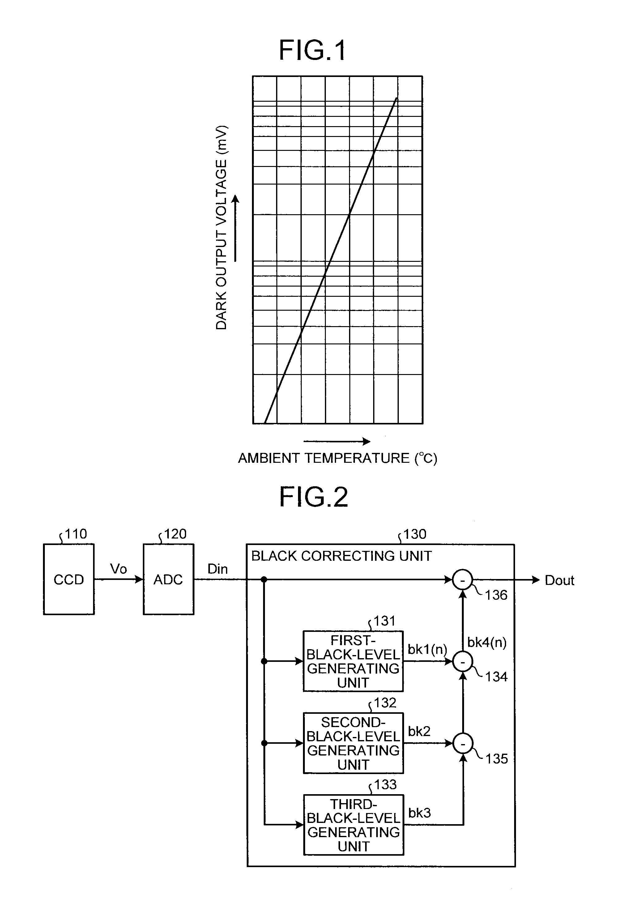
[0040]An image scanning device according to a first embodiment is described below based on the characteristic of the dark current described above and the conventional black correction method. The image scanning device according to the first embodiment is configured to perform black correction in a manner described below. Electric signal output from a photoelectric conversion unit is converted into digital image data. Pixel-by-pixel black levels of a pixel contained in pre-scanning digital image data, which is obtained before an original document is scanned, are corrected based on a ratio of a dark-current black level of the pixel contained in ongoing-scanning digital image data, which is obtained during scanning of the original, to a dark-current black level of the pixel contained in the pre-scanning digital image data. The corrected pixel-by-pixel black levels are subtracted from the ongoing-scanning digital image data.

[0041]FIG. 5 is a block diagram illustrating a functional confi...

second embodiment

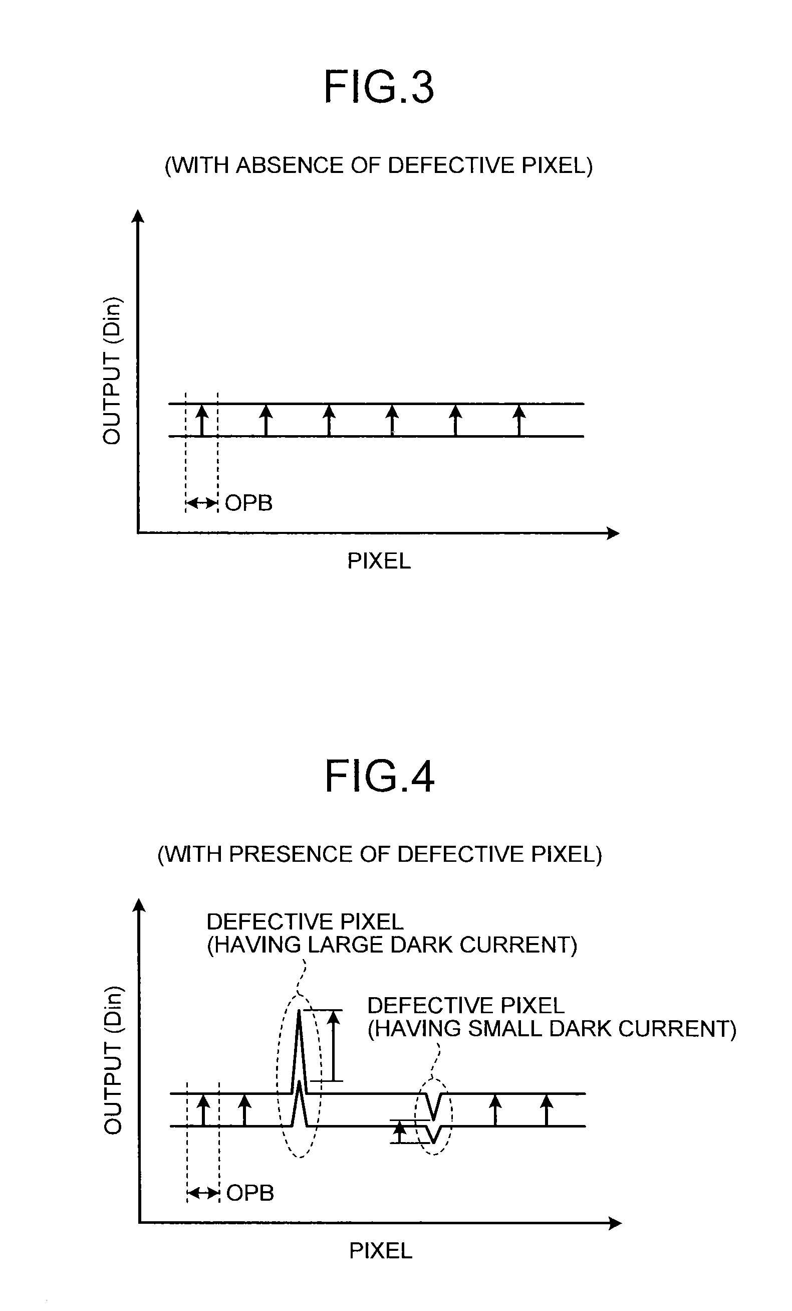
[0057]In the first embodiment described above, it is assumed that temperature distribution among the pixels of the CCD 1 is uniform. However, there can be case where the temperature distribution becomes nonuniform in a direction in which the pixels are arranged due to heat from an output circuit when the photoelectric transducer, such as the CCD 1, is operated at high speed. (For instance, in a CCD, an output circuit is generally arranged at one end of an array of pixels. Accordingly, temperatures of pixels near the output circuit are higher.) When the temperature distribution is nonuniform due to such variation in temperature among the pixels, temporal change in black level cannot be correct properly.

[0058]FIG. 9 is a schematic diagram illustrating temperature distribution among pixels. FIG. 10 is a schematic diagram illustrating black levels of pixels that contain defective pixels and have the temperature distribution illustrated in FIG. 9.

[0059]Referring to the temperature distri...


PUM


Abstract

According to an embodiment, an image scanning device includes: a light source unit that emits light onto an original to be scanned; a photoelectric conversion unit that converts light from the original to an electric signal; a converting unit that converts the electric signal from the photoelectric conversion unit into digital image data; and a black correcting unit that performs black correction by correcting pixel-by-pixel black levels of pixels contained in pre-scanning digital image data obtained before the original is scanned based on a ratio of a dark-current black level of a pixel contained in ongoing-scanning digital image data obtained during scanning of the original to a dark-current black level of the pixel contained in the pre-scanning digital image data, and subtracting the corrected pixel-by-pixel black levels from the ongoing-scanning digital image data.

Description

CROSS-REFERENCE TO RELATED APPLICATIONS[0001]The present application claims priority to and incorporates by reference the entire contents of Japanese Patent Application No. 2012-165250 filed in Japan on Jul. 25, 2012.BACKGROUND OF THE INVENTION[0002]1. Field of the Invention[0003]The present invention relates generally to image scanning devices and image forming apparatuses.[0004]2. Description of the Related Art[0005]Conventional image scanning devices may perform photoelectric conversion of light (reflection light) reflected from an original document using a photoelectric transducer, such as a charge coupled device (CCD) image sensor, to generate an image signal representing an image of the original and convert the image signal into digital image data by analog-to-digital (A / D) conversion. A dark current flows through a photoelectric transducer even when light is not incident on the photoelectric transducer. Accordingly, such an image scanning device typically performs black level...

Claims


Application Information

Patent Timeline
30 Jan 2014
Publication
US20140029065A1
IPC
H04N1/407
CPC
H04N1/407; H04N1/40056
Inventors
NAKAZAWA, MASAMOTO