Device for protecting an integrated circuit against overvoltages

Active Publication Date: 2014-02-06
STMICROELECTRONICS INT NV
View PDF4 Cites 17 Cited by
  • Summary
  • Abstract
  • Description
  • Claims
  • Application Information

AI Technical Summary

Benefits of technology

[0012]An embodiment provides a device for protecting an integrated circuit against overvoltages at least partly overcoming some disadvantages of known devices.
[0013]An embodiment provides a device of protection against overvoltages, capable of protecting critical circuits, even in case of a fast overvoltage peak.

Problems solved by technology

However, a disadvantage of the device of FIG. 2 is that, in practice, unlike diodes 101 and 103 to 106 which are integrated on the same semiconductor chip, capacitor 201 is a discrete component.

Method used


Image

  • Device for protecting an integrated circuit against overvoltages
  • Device for protecting an integrated circuit against overvoltages

Examples


Embodiment Construction

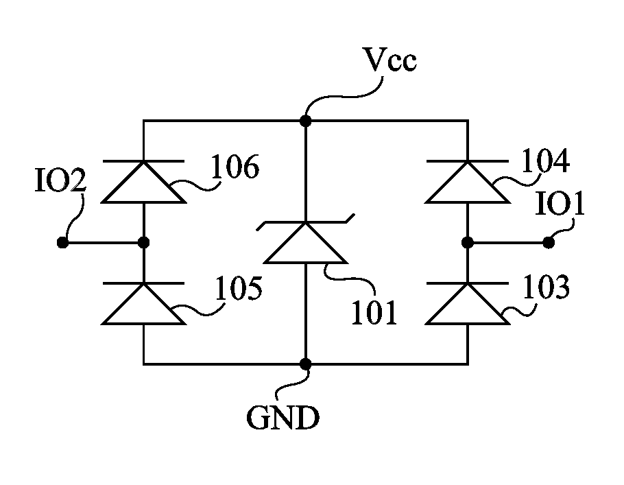
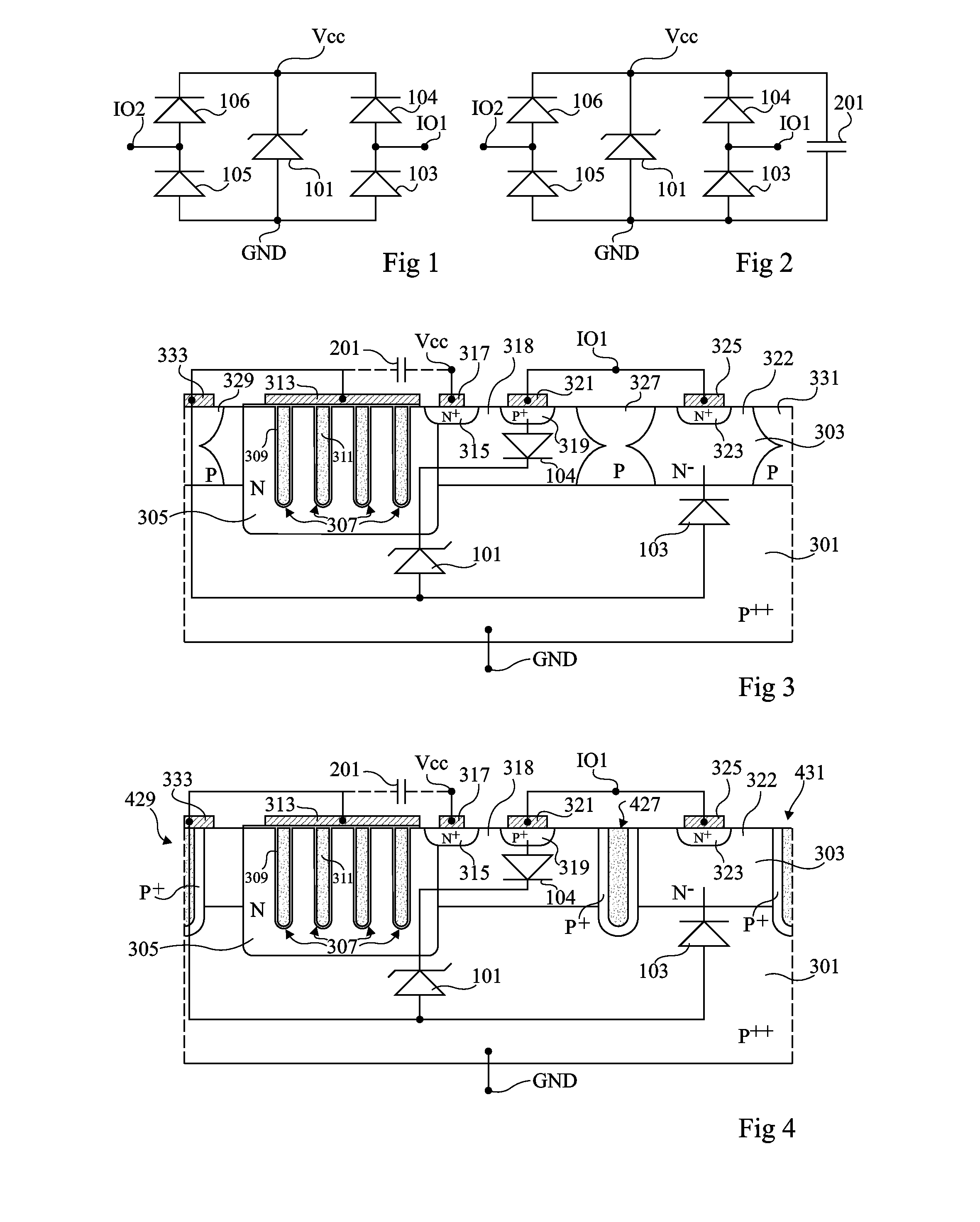
[0032]FIG. 3 is a partial simplified top view illustrating an embodiment of a device for protecting an integrated circuit (not shown) against overvoltages. The electric diagram of the protection device of FIG. 3 is the same as that of the device of FIG. 2. However, the cross-section view of FIG. 3 only shows capacitor 201, zener diode 101, and diodes 103 and 104, diodes 105 and 106 being masked by the above-mentioned components.

[0033]The protection device of FIG. 3 is formed inside and on top of a P-type doped semiconductor substrate 301, for example, a silicon substrate. In this example, substrate 301 is heavily doped (P++), and the upper surface of the substrate is coated with a lightly N-type doped epitaxial layer 303 (N−), for example, a layer having a thickness ranging between 5 and 10 μm.

[0034]In a portion of the device (left-hand portion in the orientation of the drawing), an N-type doped well 305 (N), having a heavier doping level than epitaxial layer 303, extends from the u...


PUM

PropertyMeasurementUnit
forward voltageaaaaaaaaaa
forward voltage dropaaaaaaaaaa

Abstract

A device for protecting an integrated circuit against overvoltages, the device being formed inside and on top of a semiconductor substrate of a first conductivity type and including: a capacitor including a well of the second conductivity type penetrating into the substrate and trenches with insulated walls formed in the well and filled with a conductive material; and a zener diode formed by the junction between the substrate and the well.

Description

CROSS REFERENCE TO RELATED APPLICATIONS[0001]This application claims the priority benefit of French patent application serial number 12 / 57470, filed on Aug. 1, 2012, which is hereby incorporated by reference to the maximum extent allowable by law.BACKGROUND[0002]1. Technical Field[0003]The present disclosure relates to a device for protecting an integrated circuit against overvoltages, and more specifically against electrostatic discharges.[0004]2. Discussion of the Related Art[0005]FIG. 1 is an electric diagram of an example of a device for protecting an integrated circuit against overvoltages. This device comprises a zener diode 101 having its anode connected to a low power supply terminal or rail GND of the circuit to be protected (not shown), and having its cathode connected to a high power supply terminal or rail VCC of the circuit to be protected. The device of FIG. 1 further comprises a diode 103 forward-connected between terminal GND and an input-output pad IO1 of the circui...

Claims


Application Information

Patent Timeline
Patent Type & Authority Applications(United States)
IPC IPC(8): H01L23/62
CPCH01L23/62H01L27/0255H01L2924/0002H01L2924/00
Inventor ORY, OLIVIERLACONDE, ERIC
Owner STMICROELECTRONICS INT NV
Why Eureka
Try Eureka