

Housing for wafer-level camera module
a technology of camera modules and wafers, applied in the direction of final product manufacturing, television systems, printed circuits, etc., can solve the problems of poor packaging precision, metal housings separated from the camera modules by a great spacing, and the above-mentioned design suffers from various deficiencies, so as to prevent paint from falling off and surface scratches, simple structure, and efficient cure
- Summary
- Abstract
- Description
- Claims
- Application Information
AI Technical Summary
Benefits of technology
Problems solved by technology
Method used
Image

Examples
Embodiment Construction
[0042]The above and other objectives, features and advantages of the invention will be readily apparent upon reading of following detailed description on exemplary embodiments with reference to the accompanying drawings.
[0043]Numerous specific details are set forth in the following description to provide a thorough understanding of the present invention. It will be apparent to those skilled in this art that the invention may be embodied in many different forms from the exemplary ones described hereunder and that various variants of the exemplary embodiments may be made without departing from the present teachings. Thus, the exemplary embodiments should not be construed to limit the scope of the invention.
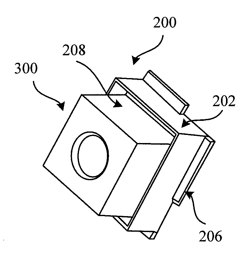
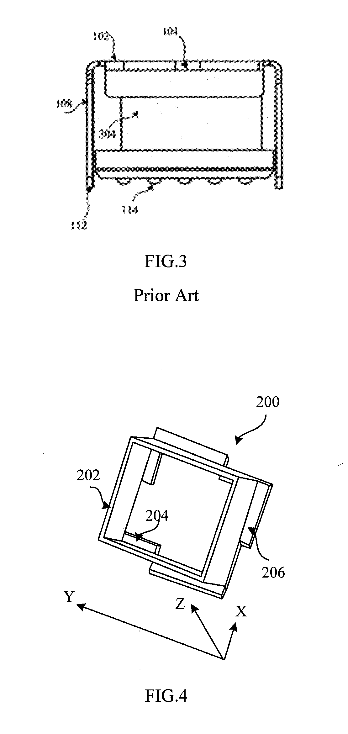
[0044]FIG. 4 shows a schematic illustration showing a housing embodying the present invention for protecting a wafer-level camera module. The housing is also configured to fix the wafer-level camera module on a PCB. The housing includes four side plates 202, four supporting plates 2...
PUM
 Abstract
Description
Claims
Application Information