Light emitting device, lighting device

a technology of light emitting device and light source, which is applied in the direction of semiconductor devices for light sources, non-metallic protective coating applications, lighting and heating apparatus, etc., can solve the problems of low spatial mixed color performance, easy color unevenness, and inability to increase the integration degree of a plurality of led devices, etc., to achieve easy light emission, easy adjustment, and high mixed color performance

Active Publication Date: 2014-04-10
CITIZEN ELECTRONICS CO LTD
View PDF5 Cites 54 Cited by
  • Summary
  • Abstract
  • Description
  • Claims
  • Application Information

AI Technical Summary

Benefits of technology

[0025]As above described, the light-emitting device of the present invention has the configuration in which each of the plurality of light-emitting sections is not formed in an agglomerated shape but is formed so that a certain one of the plurality of light-emitting sections is entangled in another one of the plurality of light-emitting sections (e.g., the plurality of light-emitting sections are formed in a spiral pattern or a striped pattern). It is therefore possible to obtain a higher mixed color performance, and it is also possible to easily emit light whose color can be easily adjusted and which has a high color rendering properly.

Problems solved by technology

However, according to the conventional techniques, a degree of integration of a plurality of LED devices cannot be increased because of a restriction such as a size of packaged components, and accordingly a spatial mixed color performance is low.
This causes a problem that the plurality of LED devices are more likely to emit respective bright spot lights, and therefore color unevenness easily occurs.
Further, a spatial mixed color performance of the light of color A and the light of color B is low.
This causes the LED devices more likely to emit respective bright spot lights, and therefore color unevenness easily occurs (e.g., shadows of an object become different colors).
Note that this problem occurs even in a case where the LED device 951 and the LED device 953 emit lights of identical colors.

Method used


Image

  • Light emitting device, lighting device
  • Light emitting device, lighting device
  • Light emitting device, lighting device

Examples


embodiment 1

Configuration of Light-Emitting Device

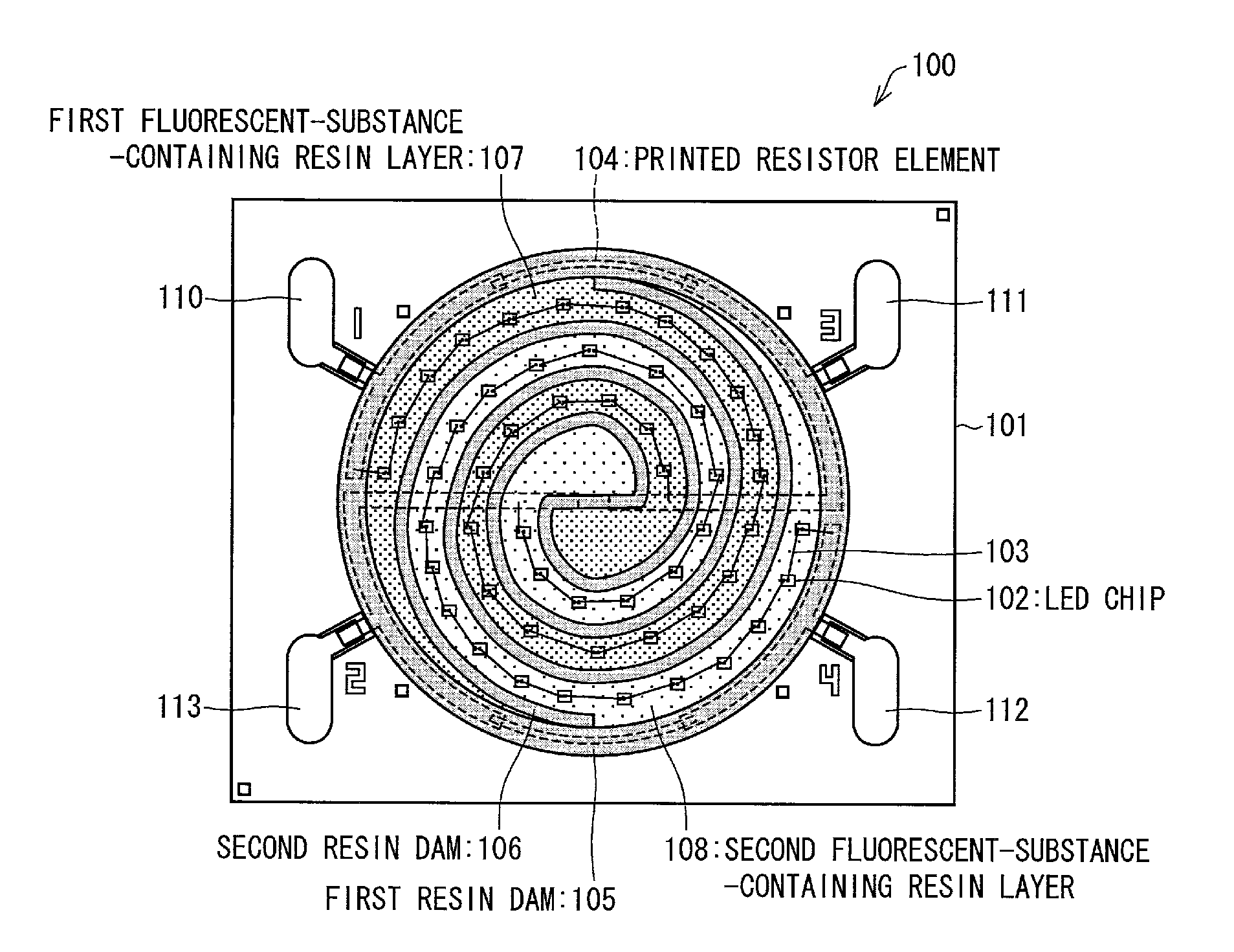
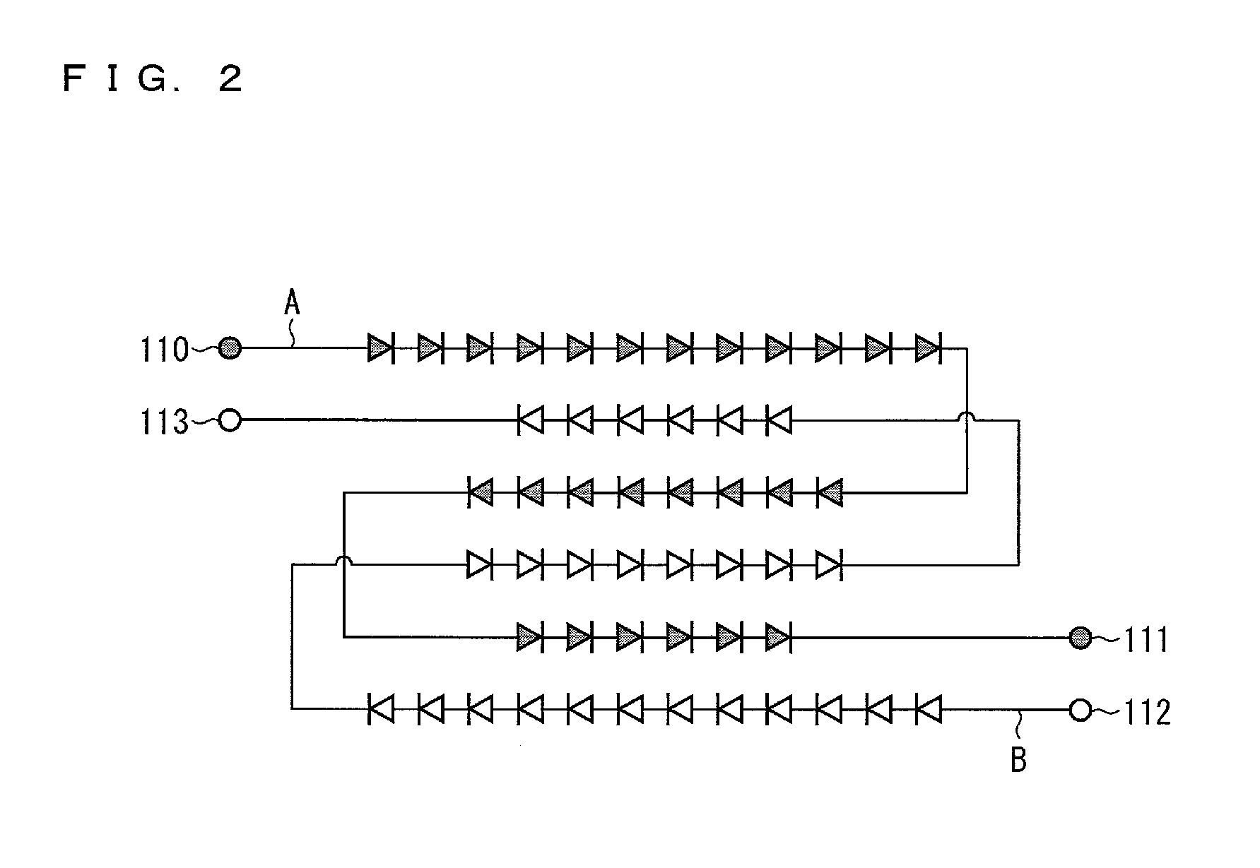
[0067]FIG. 1 is a plan view illustrating an example configuration of a light-emitting device 100 of Embodiment 1. FIG. 2 is a view illustrating a circuit configuration of LED chips 102 in the light-emitting device 100. FIGS. 3 through 6 are plan views each illustrating a configuration in manufacturing the light-emitting device 100. FIG. 3 illustrates a configuration in which an electrode wiring pattern and printed resistor elements 104 have been formed on a substrate 101. FIG. 4 illustrates a configuration in which the LED chips 102 have been mounted. FIG. 5 illustrates a configuration in which a first resin dam 105 and a second resin dam 106 have been formed. FIG. 6 illustrates a configuration in which a first fluorescent-substance-containing resin layer 107 has been formed.

[0068]The light-emitting device 100 includes a substrate 101, LED chips 102 (light-emitting element), printed resistor elements 104 (protection element), a first resin dam 1...

embodiment 2

[0140]FIG. 8 is a plan view illustrating a configuration example of a light-emitting device 200 in accordance with Embodiment 2. FIG. 9 is a view illustrating a circuit configuration of LED chips 102 in the light-emitting device 200. Each of FIGS. 10 through 13 is a plan view illustrating a configuration in manufacturing the light-emitting device 200. FIG. 10 illustrates a configuration in which an electrode wiring pattern has been formed on the substrate 101. FIG. 11 illustrates a configuration in which LED chips 102 have been mounted. FIG. 12 illustrates a configuration in which a first resin dam 105 has been formed. FIG. 13 illustrates a configuration in which a first fluorescent-substance-containing resin layer 201 has been formed.

[0141]The light-emitting device 200 includes a substrate 101, LED chips 102, a first resin dam 105, a first fluorescent-substance-containing resin layer 201 (resin layer), and a second fluorescent-substance-containing resin layer 202 (resin layer) (see...

embodiment 3

[0190]FIG. 14 is a plan view illustrating a configuration example of a light-emitting device 300 in accordance with Embodiment 3. FIG. 15 is a view illustrating a circuit configuration of LED chips 102 in the light-emitting device 300. FIG. 16 is a plan view illustrating a configuration in which the LED chips 102 are provided in manufacturing the light-emitting device 300.

[0191]The light-emitting device 300 of Embodiment 3 has a configuration which is substantially identical with that of the light-emitting device 200 of Embodiment 2, except for the following points.

[0192]That is, the light-emitting device 300 includes a plurality of LED chips 102 which are electrically connected with each other as illustrated in FIG. 15. The light-emitting device 300 includes (i) a series-parallel circuit section in which 48 LED chips 102 are connected with each other in a series-parallel manner (i.e., 4 pairs of parallel lines, in each of which 6 LED chips are connected in series, are connected in ...


PUM


Abstract

The light-emitting device includes a substrate and a plurality of light-emitting sections. A first light-emitting section is made up of LED chips and a first fluorescent-substance-containing resin layer, and a second light-emitting section is made up of LED chips and a second fluorescent-substance-containing resin layer. The first fluorescent-substance-containing resin layer and the second fluorescent-substance-containing resin layer are provided in a plurality of locations such that the fluorescent-substance-containing resin layers for the different light-emitting sections are adjacently arranged.

Description

TECHNICAL FIELD[0001]The present invention relates to a light-emitting device including an LED (Light Emitting Diode), a lighting device, and a method for manufacturing the light-emitting device. In particular, the present invention relates to a technique to generate white light which is remarkably excellent in color rendering property and in mixed color performance.BACKGROUND ART[0002]In recent years, as environmental measures against global warming, LEDs have rapidly been used as light sources of general lighting apparatuses and as light sources of backlights provided in TVs. Such a light source is configured by an LED lighting module (light-emitting device) that is configured to emit white light. Examples of a method for generating white light with the use of an LED encompass (i) a method in which white light is generated by combining the three primary colors of light with the use of three LEDs, i.e., a red LED, a blue LED, and a green LED and (ii) a method in which white light i...

Claims


Application Information

Patent Timeline
Patent Type & Authority Applications(United States)
IPC IPC(8): F21K99/00F21V23/00H05B44/00
CPCF21V23/001F21K9/50H05K1/0274H05K1/11H01L33/508H01L25/0753H01L2224/48137H01L2924/3025F21K9/232H05K2203/049H05K3/28H05K2201/10106H05K2201/09909F21Y2101/00F21V3/00H05B47/19H05B45/20F21Y2115/10H01L2924/00F21V29/77F21K9/64F21K9/68F21K9/235F21K9/237F21V3/02
Inventor HATA, TOSHIOAGATANI, MAKOTOUEMURA, TOYONORIISHIZAKI, SHINYAMATSUSHITA, HITOSHI
Owner CITIZEN ELECTRONICS CO LTD
Why Eureka
Try Eureka