Electro-optical modulator interface

a technology of optical modulator and interface, applied in the direction of optics, instruments, electrical equipment, etc., can solve the problems of tens of ghz relying on relatively expensive, subject to safe operating area (soa) issues, etc., and achieve the effect of low cost, low cost and low cost of such devices

Active Publication Date: 2014-04-17
STMICROELECTRONICS INT NV
View PDF2 Cites 21 Cited by
  • Summary
  • Abstract
  • Description
  • Claims
  • Application Information

AI Technical Summary

Benefits of technology

This patent describes how to make electronic components called E-O interfaces and associated circuits using standard semiconductor processes like CMOS. By doing this, it becomes possible to create these components more efficiently and cheaperly. However, there are some challenges that have to be solved first: namely, ensuring good performance even when driving the reversed parts of the component's structure requires overcoming certain technical problems without compromising its overall efficiency or speed.

Problems solved by technology

The technical problem addressed in this patent text relates to designing a high-speed electric-optical interface's driver component, which converts an electrical signal into an optical signal. This driver needs to provide enough power to operate the modulator while also reducing its own power consumption. Additionally, there can be challenges related to programming the timing of the driver stages to ensure optimal performance. The text discusses different solutions that have been developed over the past decade using various techniques like traveling waves, amplifiers, and MOS transistors.

Method used


Image

  • Electro-optical modulator interface
  • Electro-optical modulator interface
  • Electro-optical modulator interface

Examples


Embodiment Construction

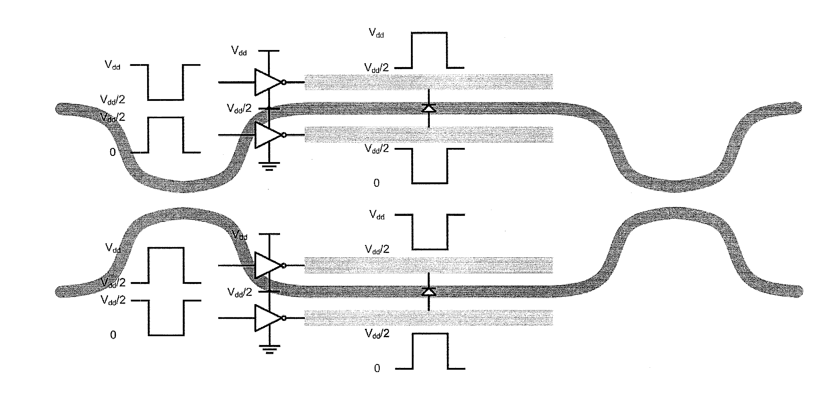
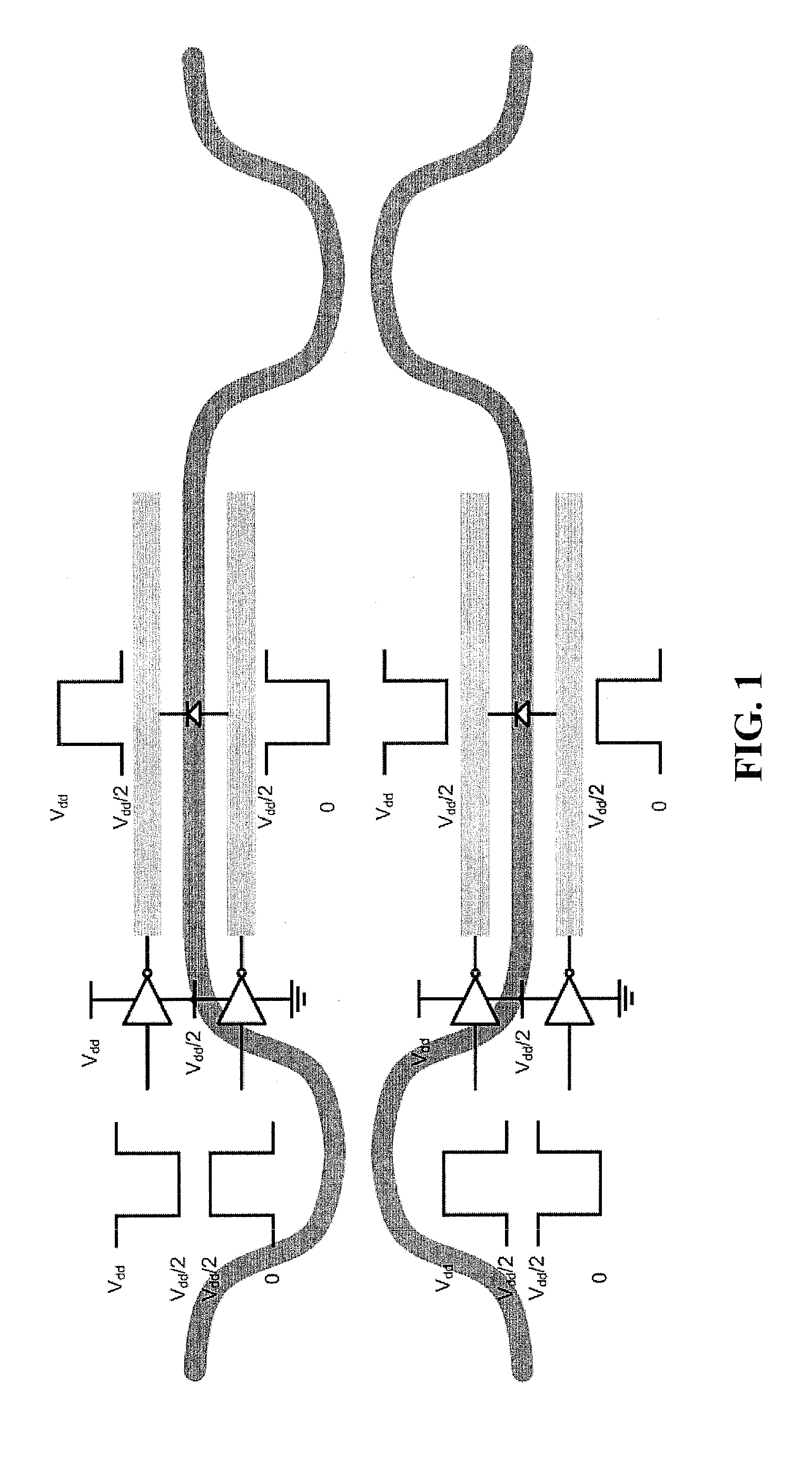
[0022]Exemplary embodiments of the driver will be described in a differential configuration, according to which all the four electrodes are driven, with either a lumped or distributed structure. This configuration may be useful, for example, in an MZM where all the four electrodes are driven as depicted in FIG. 1, and it may be more easily converted into a single-ended one, for use in an MZM where only two electrodes are driven as depicted in FIG. 2.

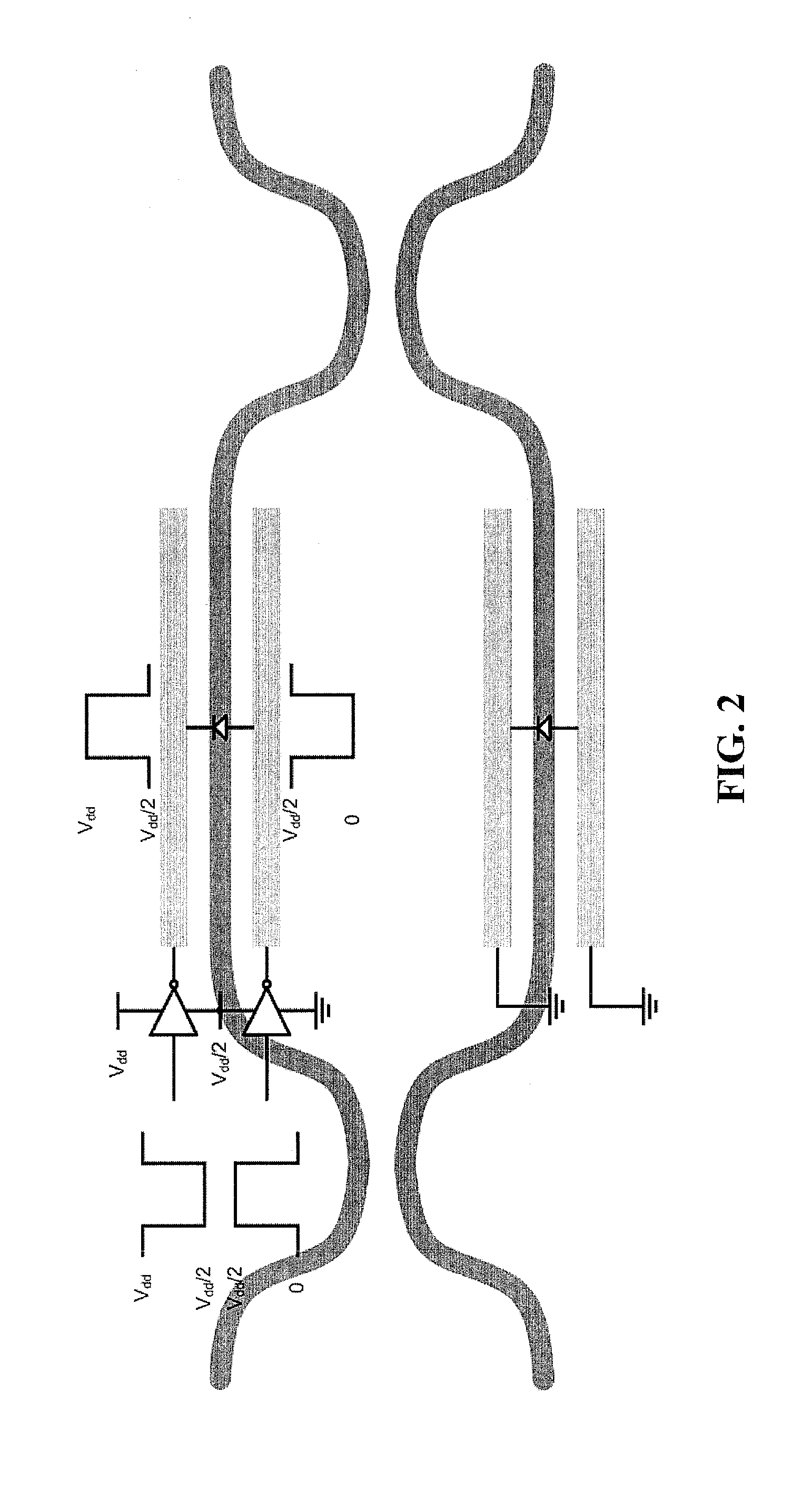
[0023]FIGS. 3a-3d are schematic diagrams of several embodiments of the E-O interface driver of this disclosure. With reference to FIG. 3a, in a case of an OOK input signal on the differential input nodes INP and INM, the driver provides a differential voltage equal to 0 or to Vdd between the two terminals of each load Cload1 and Cload2 (to the cathode and the anode in the case of a reverse biased junction) that are driven as a function of the signal pairs INM_H-INP_L and INP_H-INM_L generated in a pre-driver stage, in phase opposition. E...


PUM


Abstract

A relatively high-speed, high-efficiency CMOS two branch driver core that may operate under relatively low supply voltage may include thin oxide CMOS transistors configured to generate rail-to-rail output swings larger than twice a supply voltage and without exceeding safe operating area limits. Each of the two branches may include two stacked CMOS inverter pairs configured to drive a respective load capacitance coupled between respective CMOS inverter outputs, in phase opposition to the other branch. A pre-driver circuit input with a differential modulating signal may output two synchronous differential voltage drive signals of a swing of half of the supply voltage and DC-shifted by half of the supply voltage with respect to each other and that may be applied to the respective CMOS inverter inputs of the two branches.

Description


Claims


Application Information

Patent Timeline
Owner STMICROELECTRONICS INT NV
Why Eureka
Try Eureka