Display device and bonding test system

a technology of bonding test and display device, which is applied in the field of display devices, can solve the problems of disadvantageous increase of bumps or pins in the contemporary display device, deterioration of display device functions, etc., and achieve the effect of reducing the number of dedicated bumps

Active Publication Date: 2014-05-01
SAMSUNG DISPLAY CO LTD
View PDF9 Cites 19 Cited by
  • Summary
  • Abstract
  • Description
  • Claims
  • Application Information

AI Technical Summary

Benefits of technology

[0009]Embodiments of the present invention provide a display device capable of reducing the number of dedicated bumps for bonding resistance measurement.

Problems solved by technology

When the bonding resistance is increased due to a COG process variation, an IC bump shape, a pad resistance variation or the like, functions of the display device may deteriorate.
Since additional bumps are formed to measure the bonding resistance, the number of bumps or pins is disadvantageously increased in the contemporary display device.

Method used


Image

  • Display device and bonding test system
  • Display device and bonding test system
  • Display device and bonding test system

Examples


Embodiment Construction

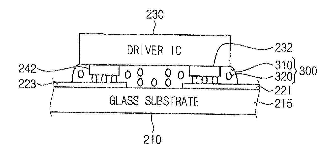
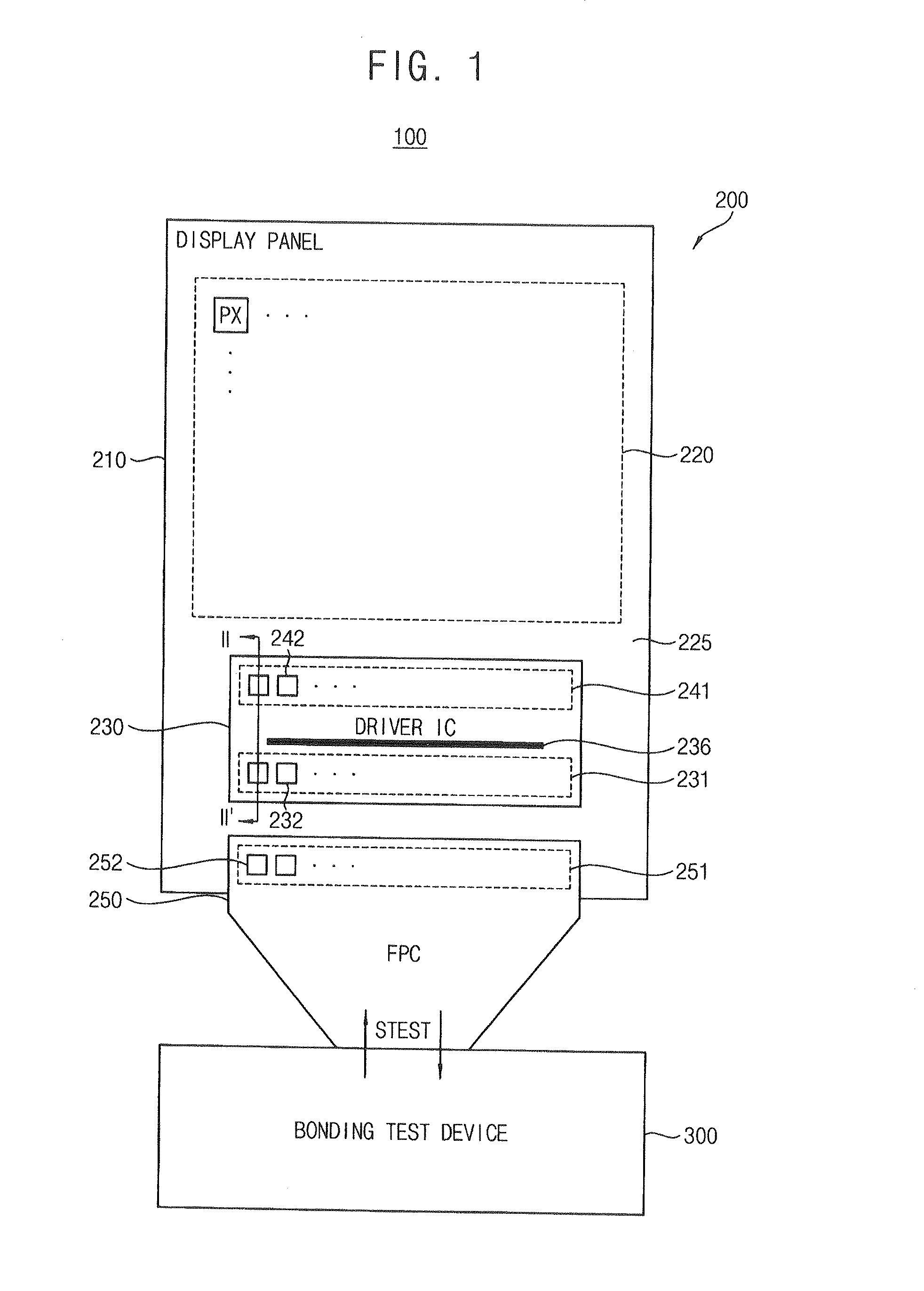
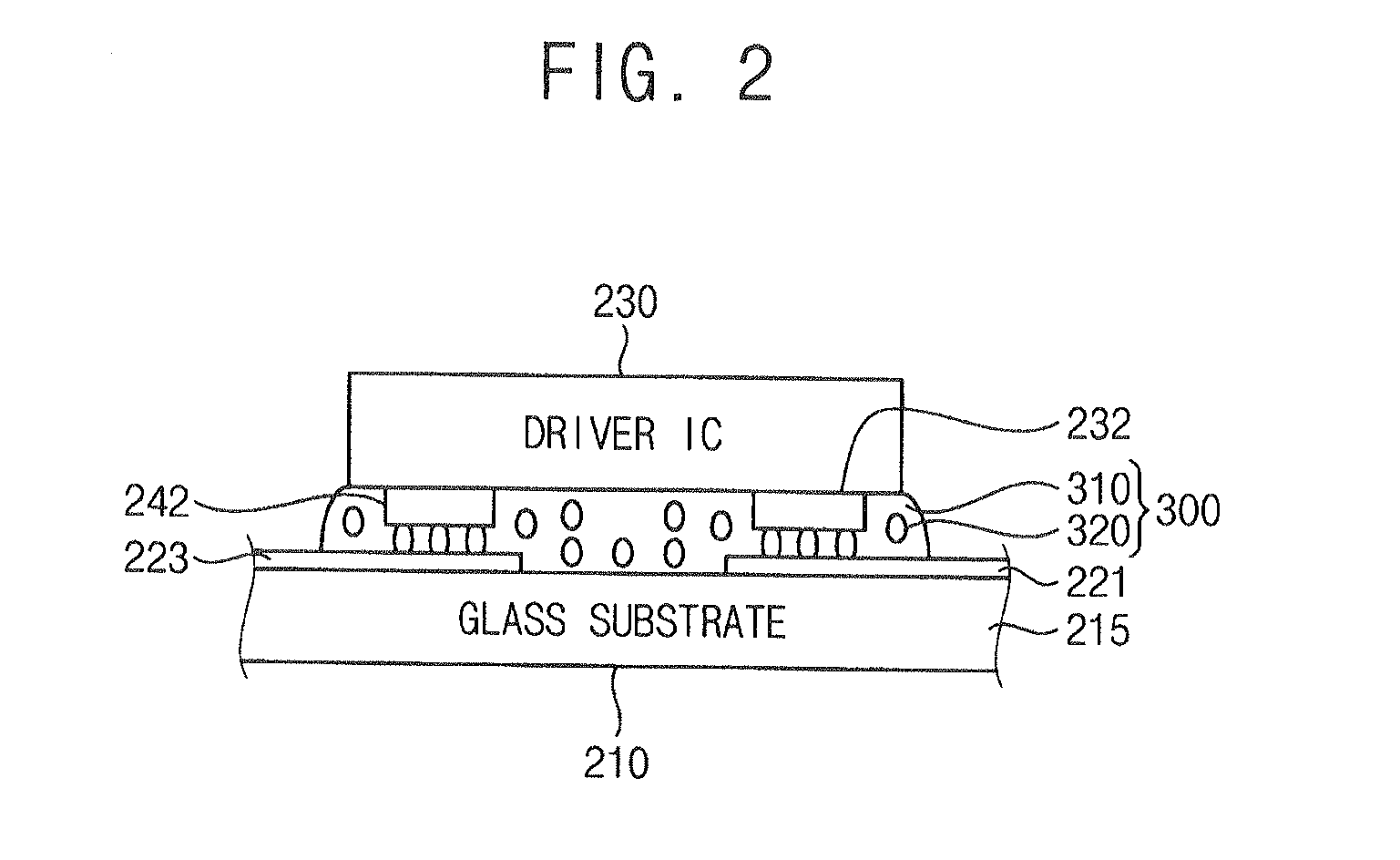
[0041]The example embodiments are described more fully hereinafter with reference to the accompanying drawings. The inventive concept may, however, be embodied in many different forms and should not be construed as limited to the example embodiments set forth herein. In the drawings, the sizes and relative sizes of layers and regions may be exaggerated for clarity.

[0042]It will be understood that when an element or layer is referred to as being “on,”“connected to” or “coupled to” another element or layer, it can be directly on, connected or coupled to the other element or layer or intervening elements or layers may be present. In contrast, when an element is referred to as being “directly on,”“directly connected to” or “directly coupled to” another element or layer, there are no intervening elements or layers present. Like or similar reference numerals refer to like or similar elements throughout. As used herein, the term “and / or” includes any and all combinations of one or more of ...


PUM


Abstract

A display device includes a display panel having a glass substrate, a first input pad formed on the glass substrate and a second input pad formed on the glass substrate, and a driver integrated circuit mounted on the glass substrate of the display panel using a chip-on-glass (COG) method. The driver integrated circuit includes first and second input bumps respectively coupled to the first and second input pads, and an internal ground line coupled to the first and second input bumps. The first input bump of the driver IC receives a test signal through the first input pad when a COG bonding test is performed, and receives a ground voltage when the display device operates.

Description

CLAIM OF PRIORITY[0001]This application makes reference to, incorporates the same herein, and claims all benefits accruing under 35 U.S.C. §119 from an application earlier filed in the Korean Intellectual Property Office on 1 Nov. 2012 and there duly assigned Serial No. 10-2012-0122854.BACKGROUND OF THE INVENTION[0002]1. Field of the Invention[0003]An embodiment of the present invention relates to display devices, and more particularly, to display devices where chip-on-glass (COG) / film-on-glass (FOG) bonding tests are performed and to the bonding test systems.[0004]2. Description of the Related Art[0005]In a display device, a driver integrated circuit (IC) may be mounted on a display panel using a chip-on-glass (COG) method, a tape carrier package (TCP) method, a chip-on-film (COF) method, etc. In comparison with the TCP method and the COF method, the COG method is simpler and may increase the relative size of a displaying region in the display panel. Therefore, the COG method is re...

Claims


Application Information

Patent Timeline
Patent Type & Authority Applications(United States)
IPC IPC(8): G01R31/02
CPCG01R31/02G09G3/006G02F1/1345G09F9/00G09G3/20
Inventor HWANG, KYUNG-HOLEE, DONG-HWAN
Owner SAMSUNG DISPLAY CO LTD
Why Eureka
Try Eureka