
Optical Tilted Charge Devices And Techniques

a charge device and optical technology, applied in the direction of electric light circuit arrangement, basic electric elements, electric apparatus, etc., can solve the problems of low electrical input impedance, low electrical gain (lc/lb), and low efficiency of driving

Inactive Publication Date: 2014-05-29
QUANTUM ELECTRO OPTO SYST
View PDF2 Cites 7 Cited by
  • Summary
  • Abstract
  • Description
  • Claims
  • Application Information

AI Technical Summary

Benefits of technology

The patent describes methods for producing light emission using a layered semiconductor structure. The methods involve applying electrical signals to the structure to stimulate light emission from different regions. The structure includes a collector region, a base region, and emitter regions. The methods can be used to produce light emission in a more efficient and controlled manner. The patent also describes the use of quantum size regions and drain / couplers to enhance the efficiency of light emission. The technical effects of the patent include improved methods for producing light emission and increased efficiency of the process.

Problems solved by technology

However, due to the diode configuration of the device, its electrical input impedance is generally too low for efficient driving; that is, much less than the typically required 50 ohms.
However, the incorporation of the quantum well structure in the base of an optical tilted charge transistor results in low electrical gain (lc / lb), lower electrical speed (ft) and more serious emitter crowding related issues.
The lower gain and lower ft limits the usability of its electrical output port.

Method used


Image

  • Optical Tilted Charge Devices And Techniques
  • Optical Tilted Charge Devices And Techniques
  • Optical Tilted Charge Devices And Techniques

Examples


Embodiment Construction

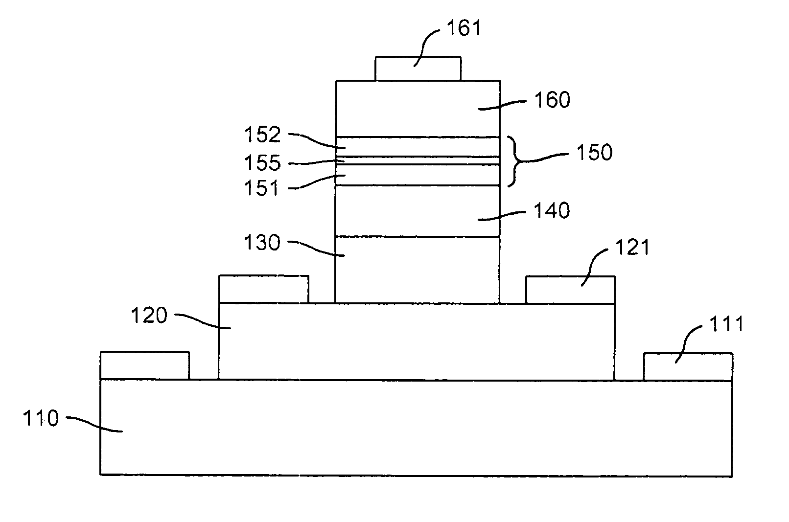
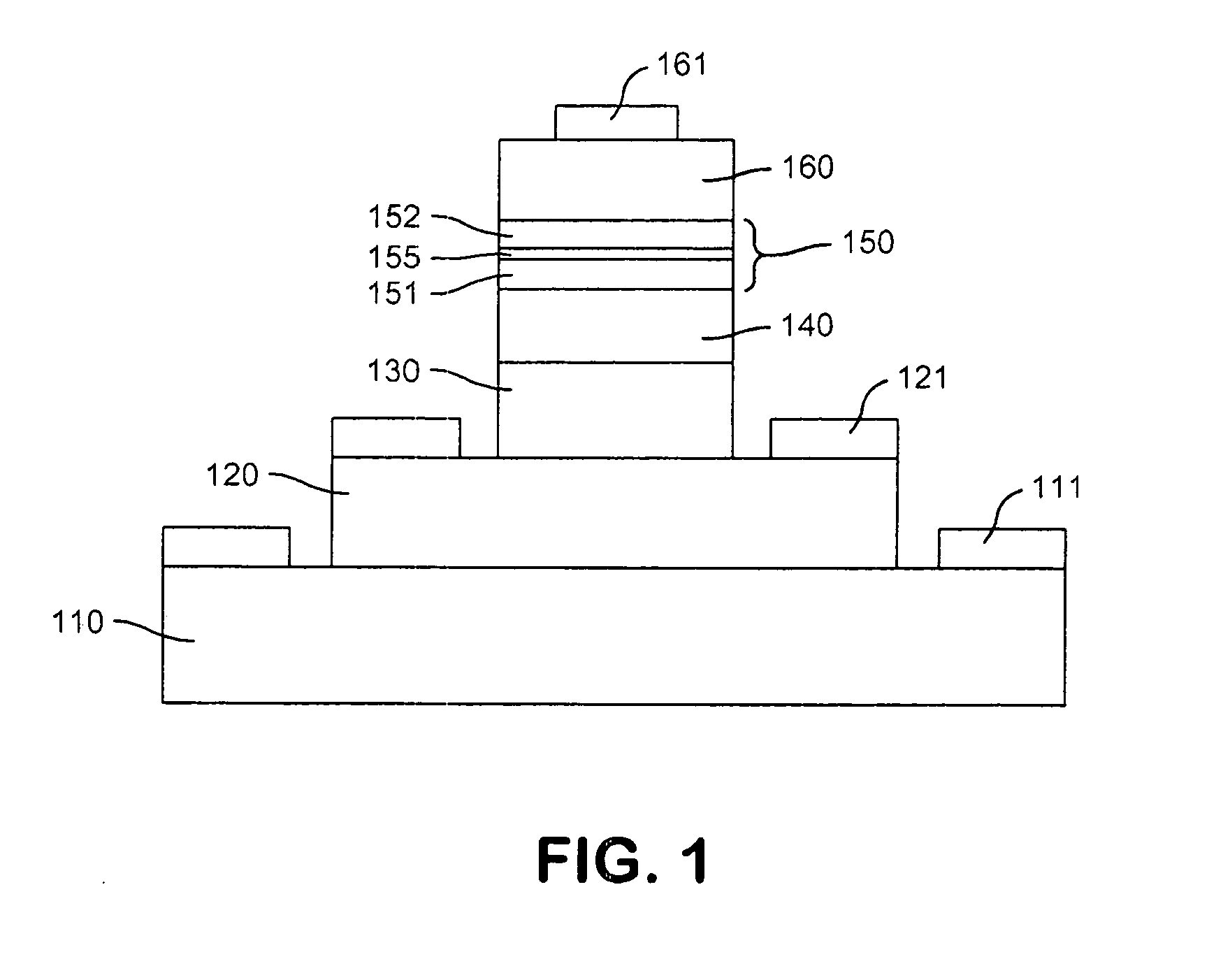
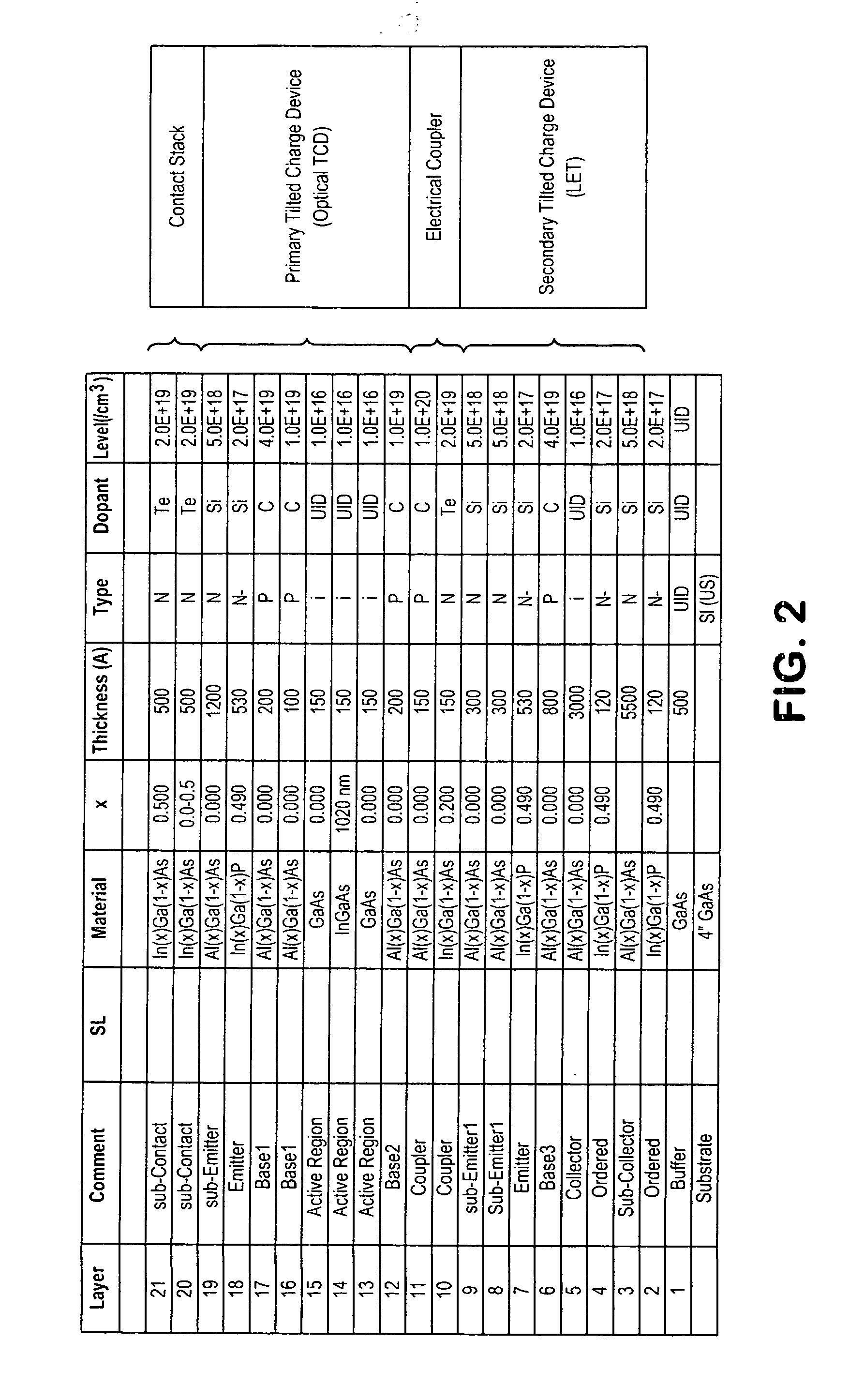
[0022]Referring to FIG. 1, there is shown a simplified cross-section of a device in accordance with an embodiment of the invention, and which can be used in practicing an embodiment of a method in accordance with the invention. The semiconductor layer structure of an example of this embodiment is shown in the table of FIG. 2. A collector region 110 has a base region 120 disposed as a mesa thereon, and an emitter region 130 is disposed as a mesa on the base region 120. A collector terminal 111 and a base terminal 121 are respectively coupled with the collector 110 and the base 120. The described collector 110, base 120, and emitter 130 of the present example are set forth in further detail in the layer table of FIG. 2, which lists a GaAs substrate and a GaAs buffer layer (1) on which the described collector 110, base 120, and emitter 130 are deposited, with the listed intervening layers and auxiliary layers. The resultant device operates as a heterojunction bipolar transistor (HBT), ...


PUM


Abstract

A method for producing light emission, including the following steps: providing a layered semiconductor structure that includes a collector region, a first base region, a first emitter region, a coupling region, a second base region, and a second emitter region; providing a quantum size region within the second base region; and applying electrical signals with respect to the second emitter region, the first base region and the collector region, to produce light emission from the second base region.

Description

PRIORITY CLAIM[0001]Priority is claimed from U.S. Provisional Patent Application No. 61 / 796,965, filed Nov. 26, 2012, and said Provisional patent application is incorporated herein by reference.FIELD OF THE INVENTION[0002]This invention relates to the field of semiconductor light emitting devices and techniques and, more particularly, to tilted charge light emitting devices and methods, including such devices and methods that have improved efficiency and manufacturability.BACKGROUND OF THE INVENTION[0003]Included in the background of the present invention are technologies relating to heterojunction bipolar transistors (HBTs, which are electrical tilted charge devices) and light-emitting transistors, transistor lasers, and tilted charge light-emitting diodes (respectively, LETs, TLs, and TCLEDs, all of which are optical tilted charge devices). A tilted charge device gets its name from the energy diagram characteristic in the device's base region, which has, approximately, a descendin...

Claims


Application Information

Patent Timeline
Patent Type & Authority Applications(United States)
IPC IPC(8): H01L33/06H01L33/32H01L33/00
CPCH01L33/06H01L33/32H01L33/0025H01L25/167H01L27/15H01L33/0016H01L33/04H01L33/30H01L2924/0002H01L2924/00
Inventor WALTER, GABRIEL
Owner QUANTUM ELECTRO OPTO SYST
Learn More