Multilayered substrate and method of manufacturing the same

Active Publication Date: 2014-07-03
SAMSUNG ELECTRO MECHANICS CO LTD
View PDF10 Cites 28 Cited by
  • Summary
  • Abstract
  • Description
  • Claims
  • Application Information

AI Technical Summary

Benefits of technology

[0017]An object of embodiments of the present invention

Problems solved by technology

Meanwhile, as the electronic component embedded substrate has been thinned, a warpage phenomenon of the substrate has become a serious problem.
As the electronic component embedded substrate has been made of various materials having different coefficients of thermal expansion, the warpage of the substrate has been intensified.
However, in the case of forming the insulating layer using only the material having high rigidity, since a surface of the insulating layer is rough, there was a limitation in improving a degree of integration of wiring patterns formed on the insulati

Method used


Image

  • Multilayered substrate and method of manufacturing the same
  • Multilayered substrate and method of manufacturing the same
  • Multilayered substrate and method of manufacturing the same

Examples


Embodiment Construction

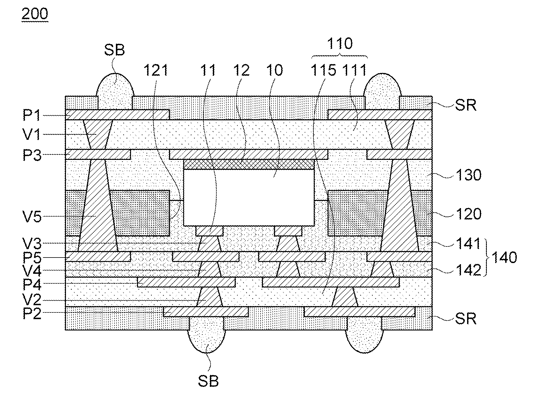
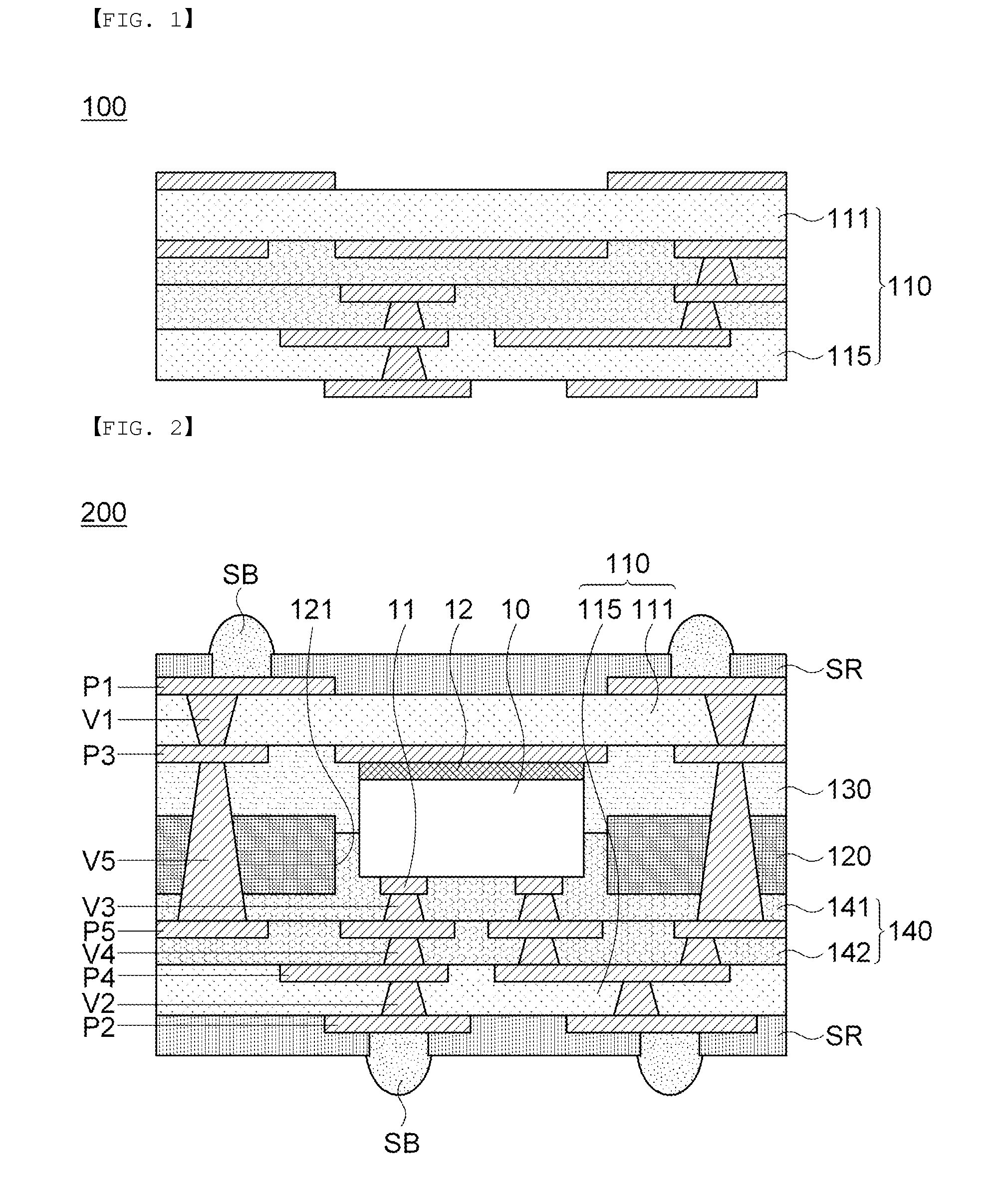
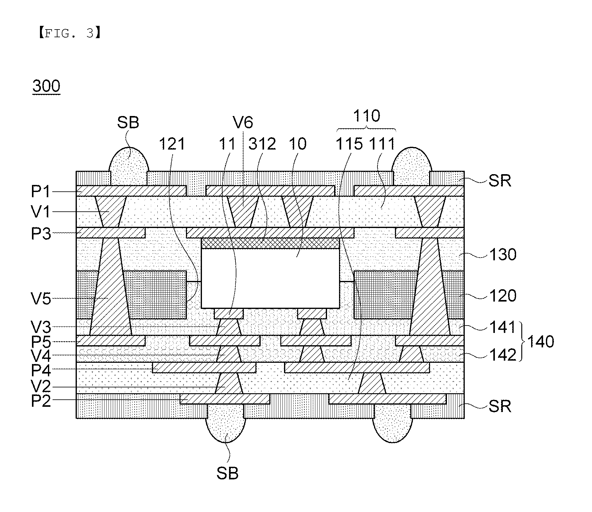
[0046]Various advantages and features of the present invention and methods accomplishing thereof will become apparent from the following description of exemplary embodiments with reference to the accompanying drawings. However, the present invention may be modified in many different forms and it should not be limited to exemplary embodiments set forth herein. These exemplary embodiments may be provided so that this disclosure will be thorough and complete, and will fully convey the scope of the invention to those skilled in the art. Like reference numerals throughout the description denote like elements.

[0047]Terms used in the present specification are for explaining exemplary embodiments rather than limiting the present invention. Unless explicitly described to the contrary, a singular form includes a plural form in the present specification. The word “comprise” and variations such as “comprises” or “comprising,” will be understood to imply the inclusion of stated constituents, ste...


PUM

PropertyMeasurementUnit
Elastic modulusaaaaaaaaaa
Temperature coefficient of resistanceaaaaaaaaaa
Coefficient of linear thermal expansionaaaaaaaaaa

Abstract

A multilayered substrate and a method of manufacturing the same. The multilayered substrate includes a plurality of wiring layers and reinforcing layers disposed at the outermost portions of both surfaces of the multilayered substrate, respectively, in order to decrease warpage of the multilayered substrate and has wiring patterns optimized depending on a scheme in which external electrodes are formed on an electronic component.

Description

CROSS REFERENCE(S) TO RELATED APPLICATIONS[0001]This application claims the foreign priority benefit under 35 U.S.C. Section 119 of Korean Patent Application Serial Nos. 10-2012-0157886 and 10-2013-0137665, filed on Dec. 31, 2012 and Nov. 13, 2013 in the Korean Intellectual Property Office, entitled “Multilayered Substrate and Method of Manufacturing the Same”, the disclosure of which is hereby incorporated by reference in its entirety.BACKGROUND[0002]1. Technical Field[0003]Embodiments of the present invention relate to a multilayered substrate and a method of manufacturing the same.[0004]2. Description of the Related Art[0005]In accordance with a trend toward lightness, miniaturization, an increase in a speed, multi-functionization, and improvement in performance of electronic devices, multilayered substrate technologies in which a plurality of wiring layers are formed on a printed circuit board (PCB) have been developed. Further, technologies in which electronic components such a...

Claims


Application Information

Patent Timeline
IPC IPC(8): H05K1/02H05K3/30H05K3/46
CPCH05K1/0271H05K3/46H05K3/30H05K1/0298H05K3/0097H05K3/4682H05K3/4688H05K2201/0175H05K2201/068H05K2203/0152H05K2203/1572H05K1/185H01L2224/12105H01L2224/73267H01L2224/04105H01L2924/15311H01L2224/19H01L2224/32225H01L2224/92244H01L21/568H01L24/19H01L2924/3511Y10T29/4913Y10T29/49155H01L2224/83005H01L24/18
Inventor LEE, DOO HWANKANG, HO SHIKSHIN, YEE NACHUNG, YUL KYOLEE, SEUNG EUN
Owner SAMSUNG ELECTRO MECHANICS CO LTD
Why Eureka
Try Eureka