Package substrate, method for manufacturing the same, and package on package substrate

a technology of packaging substrate and manufacturing method, which is applied in the direction of semiconductor devices, electrical equipment, semiconductor/solid-state device details, etc., can solve the problems of difficult mass-producing of cu posts, chemical copper adhesion doesn't meet the standards, and the range of use is very limited

Inactive Publication Date: 2014-07-03
SAMSUNG ELECTRO MECHANICS CO LTD
View PDF21 Cites 3 Cited by
  • Summary
  • Abstract
  • Description
  • Claims
  • Application Information

AI Technical Summary

Benefits of technology

[0013]The present invention has been invented in order to overcome the above-described problems and it is, therefore, an object of the present invention to provide a technique that can form a post on a build-up insulating layer without performing plating on a solder resist layer when forming the post of a package substrate.
[0014]In accordance with a first embodiment of the present invention to achieve the object, there is provided a package substrate including: an inner insulating layer; a circuit pattern layer formed on the inner insulating layer; an outer insulating layer formed on the inner insulating layer to protect the circuit pattern layer and expose portions of external and internal patterns of the circuit pattern layer; a mixed pattern layer consisting of post bumps formed on the portions of the internal patterns exposed by the outer insulating layer and outermost layer patterns formed on the portions of the external patterns exposed by the outer insulating layer; and a resist layer formed on the outer insulating layer to protect the outermost layer patterns of the mixed pattern layer and expose the outermost layer patterns by an open region.

Problems solved by technology

However, it is difficult to mass-produce the Cu post due to many problems in a manufacturing method in implementing the Cu post.
It is one of typical examples that adhesion of chemical copper doesn't meet the standards when depositing the chemical copper on solder resist (SR).
In order to overcome this problem, chemical Ni / Cu etc. is used as the chemical copper or a plasma treatment is performed on the SR surface, but since a process of removing Ni is needed or there may be a problem with packaging due to changes in characteristics of the SR surface, its range of use is very limited.
At this time, there is a problem with adhesion of chemical copper when depositing the chemical copper on the solder resist layer.
That is, there is a problem with adhesion in the plating process when forming the post on the solder resist.
In order to overcome this problem, Ni / Cu is used as the chemical copper or a plasma treatment is performed on the surface of the solder resist, but since a process of removing Ni is needed when using Ni / Cu as the chemical copper and the surface characteristics of the solder resist are changed when performing a plasma treatment, there may be a problem with packaging.

Method used


Image

  • Package substrate, method for manufacturing the same, and package on package substrate
  • Package substrate, method for manufacturing the same, and package on package substrate
  • Package substrate, method for manufacturing the same, and package on package substrate

Examples


Embodiment Construction

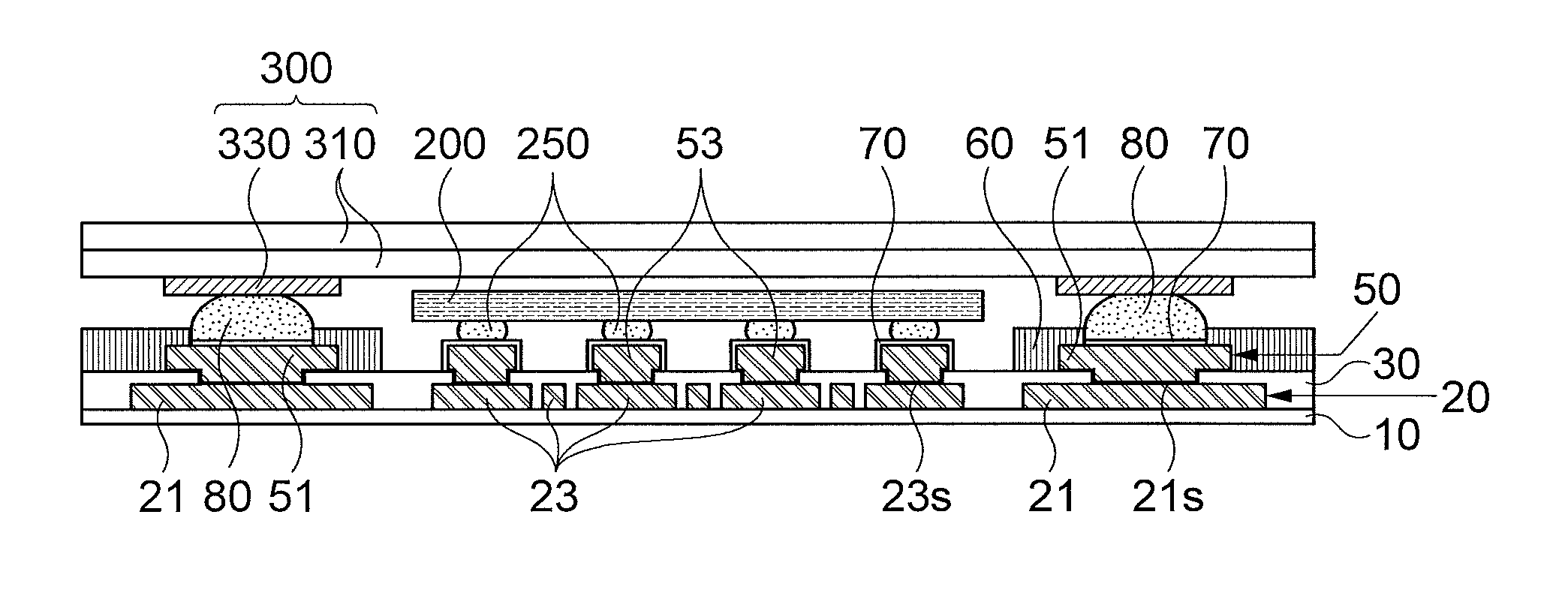
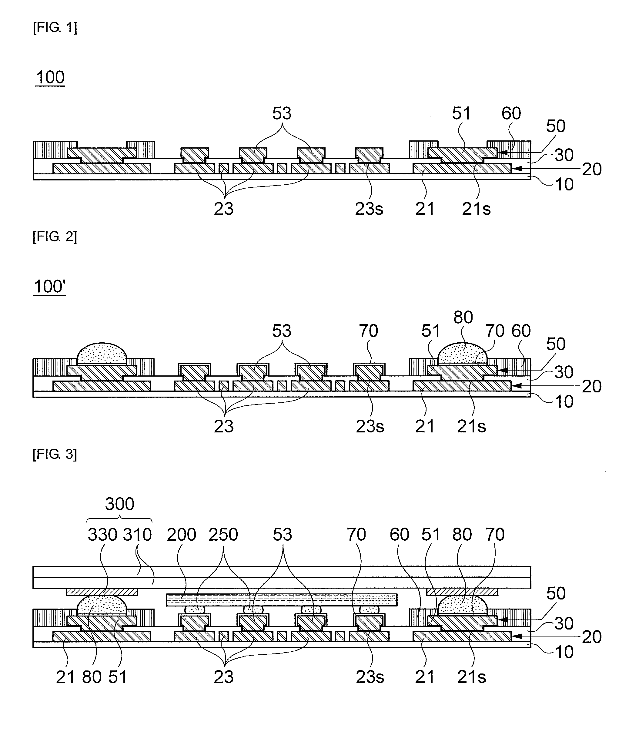
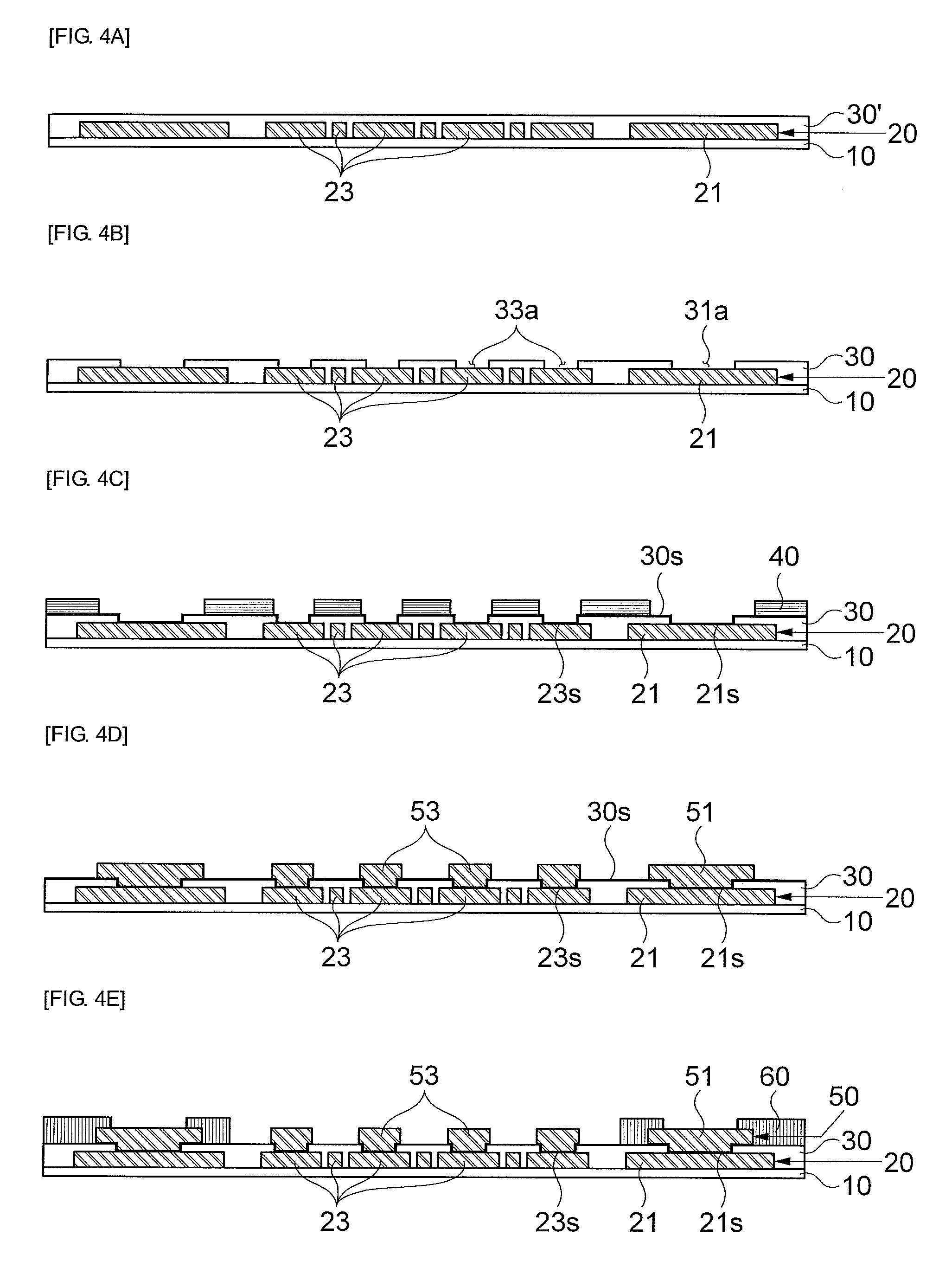
[0041]Embodiments of the present invention to achieve the above-described objects will be described with reference to the accompanying drawings. In this description, the same elements are represented by the same reference numerals, and additional description which is repeated or limits interpretation of the meaning of the invention may be omitted.

[0042]In this specification, when an element is referred to as being “connected or coupled to” or “disposed in” another element, it can be “directly” connected or coupled to or “directly” disposed in the other element or connected or coupled to or disposed in the other element with another element interposed therebetween, unless it is referred to as being “directly coupled or connected to” or “directly disposed in” the other element.

[0043]Although the singular form is used in this specification, it should be noted that the singular form can be used as the concept representing the plural form unless being contradictory to the concept of the ...


PUM


Abstract

The present invention relates to a package substrate, a method for manufacturing the same, and a package on package substrate. In accordance with an embodiment of the present invention, a package substrate including: an inner insulating layer; a circuit pattern layer formed on the inner insulating layer; an outer insulating layer formed on the inner insulating layer to protect the circuit pattern layer and expose portions of external and internal patterns of the circuit pattern layer; a mixed pattern layer consisting of post bumps and outermost layer patterns formed on the portions of the internal and external patterns exposed by the outer insulating layer; and a resist layer formed on the outer insulating layer to protect the outermost layer patterns of the mixed pattern layer and expose the outermost layer patterns by an open region.

Description

CROSS-REFERENCE TO RELATED APPLICATIONS[0001]Claim and incorporate by reference domestic priority application and foreign priority application as follows:[0002]“CROSS REFERENCE TO RELATED APPLICATION[0003]This application claims the benefit under 35 U.S.C. Section 119 of Korean Patent Application Serial No. 10-2012-0157162, entitled filed Dec. 28, 2012, which is hereby incorporated by reference in its entirety into this application.”BACKGROUND OF THE INVENTION[0004]1. Field of the Invention[0005]The present invention relates to a package substrate, a method for manufacturing the same, and a package on package substrate.[0006]2. Description of the Related Art[0007]In manufacture of printed circuit boards (PCB), since a Cu post is a kind of bump and characterized by robustness compared to a conventional Sn—Ag—Pb base bump that is easily thermally deformed, it is known to be advantageous in implementing a fine pitch. However, it is difficult to mass-produce the Cu post due to many prob...

Claims


Application Information

Patent Timeline
Patent Type & Authority Applications(United States)
IPC IPC(8): H01L23/498H01L21/768
CPCH01L21/76885H01L23/49811H01L23/49816H01L23/49822H01L23/49838H01L23/49894H01L25/105H01L2224/16225H01L2225/1023H01L2225/1058H01L2924/15321
Inventor LEE, CHANG BOCHOI, CHEOL HORYU, CHANG SUP
Owner SAMSUNG ELECTRO MECHANICS CO LTD
Why Eureka
Try Eureka